• 文献检索
  • 文档翻译
  • 深度研究
  • 学术资讯
  • Suppr Zotero 插件Zotero 插件
  • 邀请有礼
  • 套餐&价格
  • 历史记录
应用&插件
Suppr Zotero 插件Zotero 插件浏览器插件Mac 客户端Windows 客户端微信小程序
定价
高级版会员购买积分包购买API积分包
服务
文献检索文档翻译深度研究API 文档MCP 服务
关于我们
关于 Suppr公司介绍联系我们用户协议隐私条款
关注我们

Suppr 超能文献

核心技术专利:CN118964589B侵权必究
粤ICP备2023148730 号-1Suppr @ 2026

文献检索

告别复杂PubMed语法,用中文像聊天一样搜索,搜遍4000万医学文献。AI智能推荐,让科研检索更轻松。

立即免费搜索

文件翻译

保留排版,准确专业,支持PDF/Word/PPT等文件格式,支持 12+语言互译。

免费翻译文档

深度研究

AI帮你快速写综述,25分钟生成高质量综述,智能提取关键信息,辅助科研写作。

立即免费体验

通过金辅助分子束外延生长后,GaAs(111)纳米线与Si(111)衬底之间的晶格参数匹配。

Lattice parameter accommodation between GaAs(111) nanowires and Si(111) substrate after growth via Au-assisted molecular beam epitaxy.

作者信息

Davydok Anton, Breuer Steffen, Biermanns Andreas, Geelhaar Lutz, Pietsch Ullrich

机构信息

Festkörperphysik, Universität Siegen, Walter-Flex-Str, 3, Siegen, 57072, Germany.

出版信息

Nanoscale Res Lett. 2012 Feb 8;7(1):109. doi: 10.1186/1556-276X-7-109.

DOI:10.1186/1556-276X-7-109
PMID:22315928
原文链接:https://pmc.ncbi.nlm.nih.gov/articles/PMC3329407/
Abstract

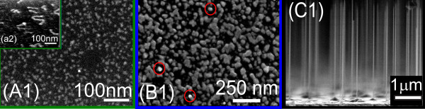
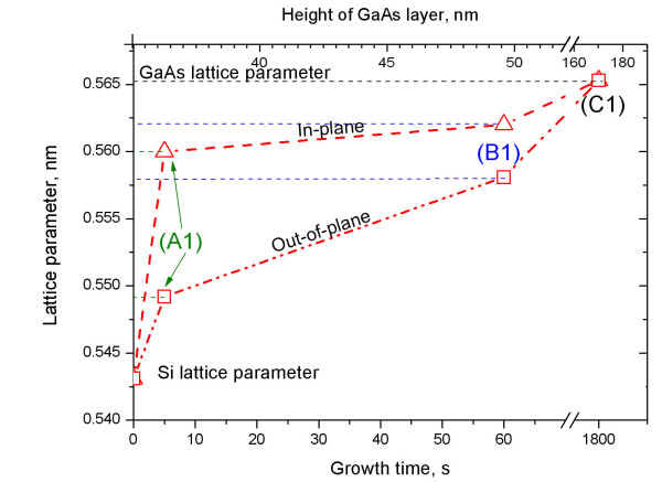
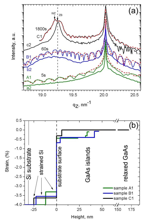
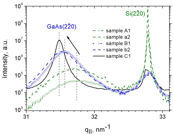
Using out-of-plane and in-plane X-ray diffraction techniques, we have investigated the structure at the interface between GaAs nanowires [NWs] grown by Au-assisted molecular beam epitaxy and the underlying Si(111) substrate. Comparing the diffraction pattern measured at samples grown for 5, 60, and 1,800 s, we find a plastic strain release of about 75% close to the NW-to-substrate interface even at the initial state of growth, probably caused by the formation of a dislocation network at the Si-to-GaAs interface. In detail, we deduce that during the initial stage, zinc-blende structure GaAs islands grow with a gradually increasing lattice parameter over a transition region of several 10 nm in the growth direction. In contrast, accommodation of the in-plane lattice parameter takes place within a thickness of about 10 nm. As a consequence, the ratio between out-of-plane and in-plane lattice parameters is smaller than the unity in the initial state of growth. Finally the wurtzite-type NWs grow on top of the islands and are free of strain.

摘要

利用面外和面内X射线衍射技术,我们研究了通过金辅助分子束外延生长的砷化镓纳米线(NWs)与下层硅(111)衬底之间界面处的结构。通过比较在生长5秒、60秒和1800秒的样品上测得的衍射图案,我们发现即使在生长的初始状态,靠近纳米线与衬底界面处也有大约75%的塑性应变释放,这可能是由于在硅与砷化镓界面处形成了位错网络所致。具体而言,我们推断在初始阶段,闪锌矿结构的砷化镓岛在生长方向上几个10纳米的过渡区域内,随着晶格参数逐渐增加而生长。相比之下,面内晶格参数的调整发生在大约10纳米的厚度范围内。因此,在生长的初始状态,面外和面内晶格参数的比值小于1。最后,纤锌矿型纳米线生长在这些岛的顶部且无应变。

https://cdn.ncbi.nlm.nih.gov/pmc/blobs/8cc5/3329407/22cbe62cbfe9/1556-276X-7-109-4.jpg
https://cdn.ncbi.nlm.nih.gov/pmc/blobs/8cc5/3329407/05708a5543d6/1556-276X-7-109-1.jpg
https://cdn.ncbi.nlm.nih.gov/pmc/blobs/8cc5/3329407/d3b3e65c99b6/1556-276X-7-109-2.jpg
https://cdn.ncbi.nlm.nih.gov/pmc/blobs/8cc5/3329407/dbb92c07f88c/1556-276X-7-109-3.jpg
https://cdn.ncbi.nlm.nih.gov/pmc/blobs/8cc5/3329407/22cbe62cbfe9/1556-276X-7-109-4.jpg

相似文献

1
Lattice parameter accommodation between GaAs(111) nanowires and Si(111) substrate after growth via Au-assisted molecular beam epitaxy.通过金辅助分子束外延生长后,GaAs(111)纳米线与Si(111)衬底之间的晶格参数匹配。
Nanoscale Res Lett. 2012 Feb 8;7(1):109. doi: 10.1186/1556-276X-7-109.
2
Strain accommodation in Ga-assisted GaAs nanowires grown on silicon (111).在硅(111)上生长的 Ga 辅助 GaAs 纳米线中的应变适应。
Nanotechnology. 2012 Aug 3;23(30):305703. doi: 10.1088/0957-4484/23/30/305703. Epub 2012 Jul 2.
3
Electrical and Optical Properties of Au-Catalyzed GaAs Nanowires Grown on Si (111) Substrate by Molecular Beam Epitaxy.通过分子束外延在Si(111)衬底上生长的金催化砷化镓纳米线的电学和光学性质
Nanoscale Res Lett. 2017 Dec;12(1):290. doi: 10.1186/s11671-017-2063-3. Epub 2017 Apr 21.
4
A Novel Growth Method To Improve the Quality of GaAs Nanowires Grown by Ga-Assisted Chemical Beam Epitaxy.一种提高 Ga 辅助化学束外延生长 GaAs 纳米线质量的新生长方法。
Nano Lett. 2018 Jun 13;18(6):3608-3615. doi: 10.1021/acs.nanolett.8b00702. Epub 2018 May 11.
5
Zinc blende GaAsSb nanowires grown by molecular beam epitaxy.通过分子束外延生长的闪锌矿结构砷化镓锑纳米线。
Nanotechnology. 2008 Jul 9;19(27):275605. doi: 10.1088/0957-4484/19/27/275605. Epub 2008 May 28.
6
Grazing-incidence X-ray diffraction of single GaAs nanowires at locations defined by focused ion beams.聚焦离子束所定义位置处单根砷化镓纳米线的掠入射X射线衍射。
J Appl Crystallogr. 2013 Aug 1;46(Pt 4):887-892. doi: 10.1107/S0021889813004226. Epub 2013 Jun 7.
7
Controlling crystal phases in GaAs nanowires grown by Au-assisted molecular beam epitaxy.通过 Au 辅助分子束外延生长控制 GaAs 纳米线的晶体相。
Nanotechnology. 2013 Jan 11;24(1):015601. doi: 10.1088/0957-4484/24/1/015601. Epub 2012 Dec 5.
8
Stages in molecular beam epitaxy growth of GaAs nanowires studied by x-ray diffraction.利用 X 射线衍射研究 GaAs 纳米线分子束外延生长的阶段。
Nanotechnology. 2010 Mar 19;21(11):115603. doi: 10.1088/0957-4484/21/11/115603. Epub 2010 Feb 22.
9
Alloy formation during molecular beam epitaxy growth of Si-doped InAs nanowires on GaAs[111]B.在砷化镓[111]B衬底上分子束外延生长硅掺杂砷化铟纳米线过程中的合金形成。
J Appl Crystallogr. 2013 Aug 1;46(Pt 4):893-897. doi: 10.1107/S0021889813010522. Epub 2013 Jun 7.
10
Wurtzite phase control for self-assisted GaAs nanowires grown by molecular beam epitaxy.分子束外延生长自辅助砷化镓纳米线的纤锌矿相控制
Nanotechnology. 2021 Apr 9;32(15):155602. doi: 10.1088/1361-6528/abda75.

引用本文的文献

1
Alloy formation during molecular beam epitaxy growth of Si-doped InAs nanowires on GaAs[111]B.在砷化镓[111]B衬底上分子束外延生长硅掺杂砷化铟纳米线过程中的合金形成。
J Appl Crystallogr. 2013 Aug 1;46(Pt 4):893-897. doi: 10.1107/S0021889813010522. Epub 2013 Jun 7.
2
Grazing-incidence X-ray diffraction of single GaAs nanowires at locations defined by focused ion beams.聚焦离子束所定义位置处单根砷化镓纳米线的掠入射X射线衍射。
J Appl Crystallogr. 2013 Aug 1;46(Pt 4):887-892. doi: 10.1107/S0021889813004226. Epub 2013 Jun 7.
3
Surface-passivated GaAsP single-nanowire solar cells exceeding 10% efficiency grown on silicon.

本文引用的文献

1
The high-resolution diffraction beamline P08 at PETRA III.PETRA III 上的高分辨率衍射光束线 P08。
J Synchrotron Radiat. 2012 Jan;19(Pt 1):30-8. doi: 10.1107/S0909049511047236. Epub 2011 Nov 30.
2
Parallel array InAs nanowire transistors for mechanically bendable, ultrahigh frequency electronics.平行阵列 InAs 纳米线晶体管,用于机械可弯曲的超高频率电子器件。
ACS Nano. 2010 Oct 26;4(10):5855-60. doi: 10.1021/nn1018329.
3
Single electron charging in optically active nanowire quantum dots.光活性纳米线量子点中的单电子充电。
在硅衬底上生长的 GaAsP 单纳米线表面钝化太阳能电池,光电转换效率超过 10%。
Nat Commun. 2013;4:1498. doi: 10.1038/ncomms2510.
Nano Lett. 2010 May 12;10(5):1817-22. doi: 10.1021/nl100520r.
4
Stages in molecular beam epitaxy growth of GaAs nanowires studied by x-ray diffraction.利用 X 射线衍射研究 GaAs 纳米线分子束外延生长的阶段。
Nanotechnology. 2010 Mar 19;21(11):115603. doi: 10.1088/0957-4484/21/11/115603. Epub 2010 Feb 22.
5
Heteroepitaxial growth of vertical GaAs nanowires on Si(111) substrates by metal-organic chemical vapor deposition.通过金属有机化学气相沉积在Si(111)衬底上垂直生长GaAs纳米线的异质外延生长。
Nano Lett. 2008 Nov;8(11):3755-60. doi: 10.1021/nl802062y. Epub 2008 Oct 28.
6
Transparent active matrix organic light-emitting diode displays driven by nanowire transistor circuitry.由纳米线晶体管电路驱动的透明有源矩阵有机发光二极管显示器。
Nano Lett. 2008 Apr;8(4):997-1004. doi: 10.1021/nl072538+. Epub 2007 Dec 11.