Im Hyungsoon, Wittenberg Nathan J, Lindquist Nathan C, Oh Sang-Hyun
Laboratory of Nanostructures and Biosensing, Department of Electrical and Computer Engineering, University of Minnesota, Minneapolis, MN 55455, United States.
J Mater Res. 2012 Feb 28;27(4):663-671. doi: 10.1557/jmr.2011.434. Epub 2012 Jan 19.
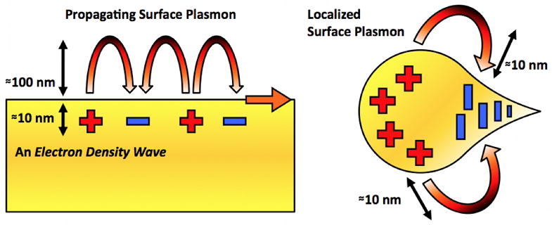
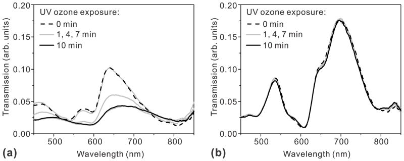
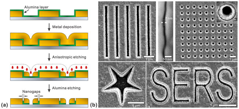
While atomic layer deposition (ALD) has been used for many years as an industrial manufacturing method for microprocessors and displays, this versatile technique is finding increased use in the emerging fields of plasmonics and nanobiotechnology. In particular, ALD coatings can modify metallic surfaces to tune their optical and plasmonic properties, to protect them against unwanted oxidation and contamination, or to create biocompatible surfaces. Furthermore, ALD is unique among thin-film deposition techniques in its ability to meet the processing demands for engineering nanoplasmonic devices, offering conformal deposition of dense and ultra-thin films on high-aspect-ratio nanostructures at temperatures below 100 °C. In this review, we present key features of ALD and describe how it could benefit future applications in plasmonics, nanosciences, and biotechnology.
虽然原子层沉积(ALD)作为微处理器和显示器的工业制造方法已使用多年,但这种多功能技术在新兴的等离子体激元学和纳米生物技术领域的应用越来越广泛。特别是,ALD涂层可以修饰金属表面,以调整其光学和等离子体激元特性,保护它们免受不必要的氧化和污染,或创建生物相容性表面。此外,ALD在薄膜沉积技术中独一无二,它有能力满足工程纳米等离子体激元器件的加工要求,能够在低于100°C的温度下在高纵横比纳米结构上实现致密和超薄膜的保形沉积。在这篇综述中,我们介绍了ALD的关键特性,并描述了它如何能使等离子体激元学、纳米科学和生物技术的未来应用受益。