Graduate School of Engineering, University of Hyogo, 2167 Shosha, Himeji 671-2280, Japan.
Sensors (Basel). 2012 Dec 4;12(12):16673-84. doi: 10.3390/s121216673.
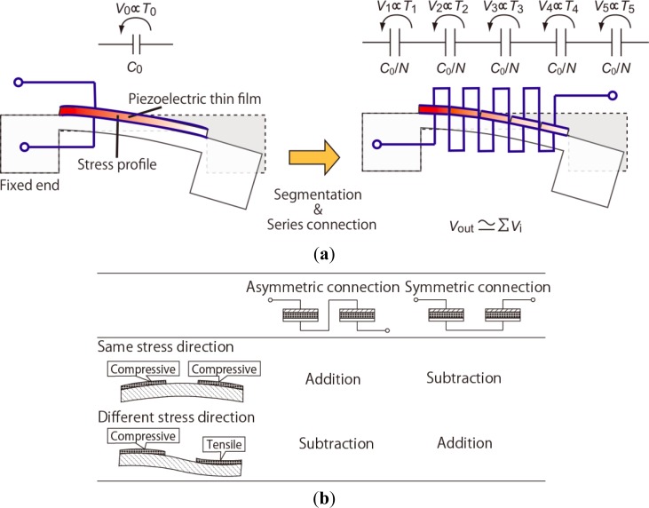
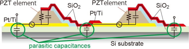
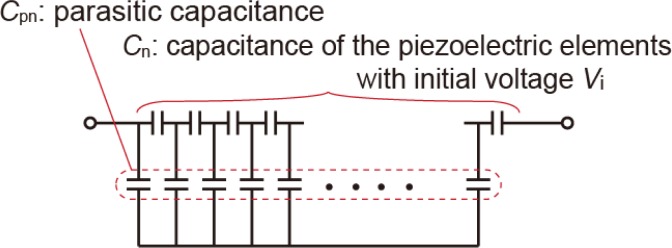
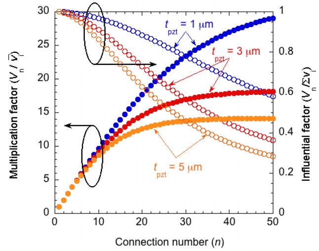
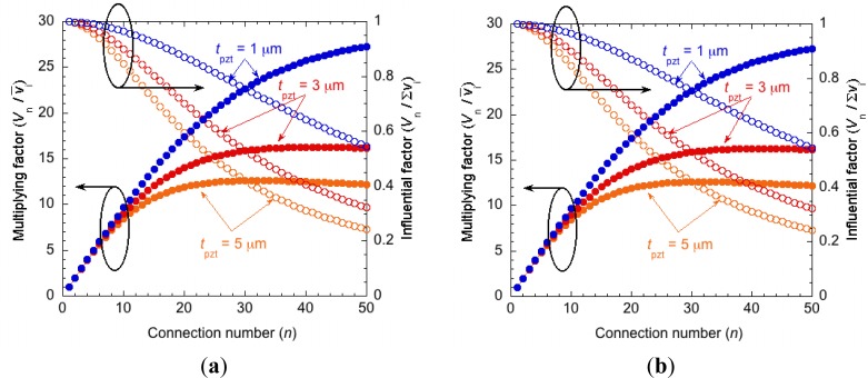
Series-connected thin film piezoelectric elements can generate large output voltages. The output voltage ideally is proportional to the number of connections. However, parasitic capacitances formed by the insulation layers and derived from peripheral circuitry degrade the output voltage. Conventional circuit models are not suitable for predicting the influence of the parasitic capacitance. Therefore we proposed the simplest model of piezoelectric elements to perform simulation program with integrated circuit emphasis (SPICE) circuit simulations). The effects of the parasitic capacitances on the thin-film Pb(Zr, Ti)O(3), (PZT) elements connected in series on a SiO(2) insulator are demonstrated. The results reveal the negative effect on the output voltage caused by the parasitic capacitances of the insulation layers. The design guidelines for the devices using series-connected piezoelectric elements are explained.
串联薄膜压电元件可以产生较大的输出电压。理想情况下,输出电压与连接数成正比。然而,由绝缘层形成并源自外围电路的寄生电容会降低输出电压。传统的电路模型不适合预测寄生电容的影响。因此,我们提出了最简单的压电元件模型,以进行集成电路重点仿真程序 (SPICE) 电路仿真。展示了在二氧化硅 (SiO2) 绝缘体上串联连接的薄膜 Pb(Zr,Ti)O3(PZT) 元件的寄生电容的影响。结果表明,绝缘层的寄生电容对输出电压有负面影响。解释了使用串联压电元件的器件的设计准则。