Alvarado Jose Alberto, Maldonado Arturo, Juarez Héctor, Pacio Mauricio, Perez Rene
Centro de Investigaciones y de Estudios Avanzados del Instituto Politecnico Nacional, programa de Nanociencias y Nanotecnología, Av. Instituto Politécnico Nacional # 2508, Col. San Pedro Zacatenco, C.P. 07360, México, D. F., México.
Centro de Investigaciones y de Estudios Avanzados del Instituto Politécnico Nacional, Sección de Electrónica del Estado Solido, Av. Instituto Politécnico Nacional # 2508, Col. San Pedro Zacatenco, C.P. 07360, México, D. F., México.
Beilstein J Nanotechnol. 2015 Apr 16;6:971-5. doi: 10.3762/bjnano.6.100. eCollection 2015.
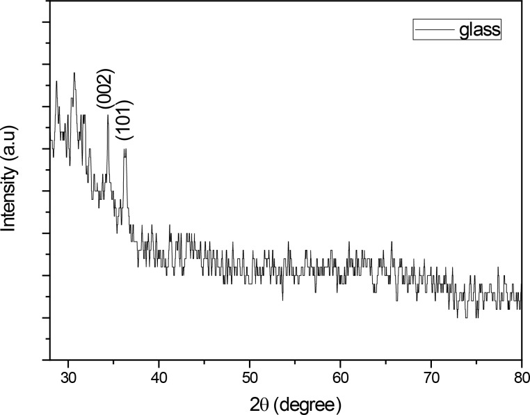
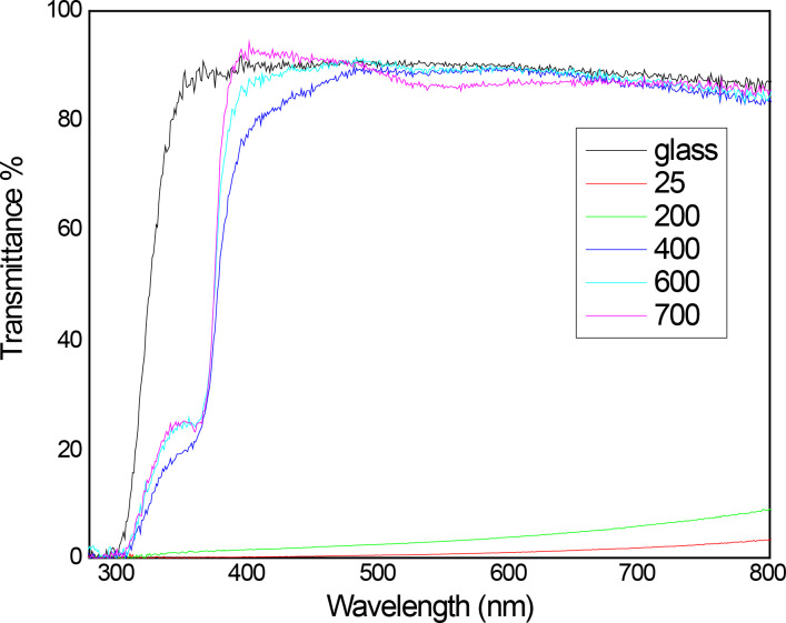
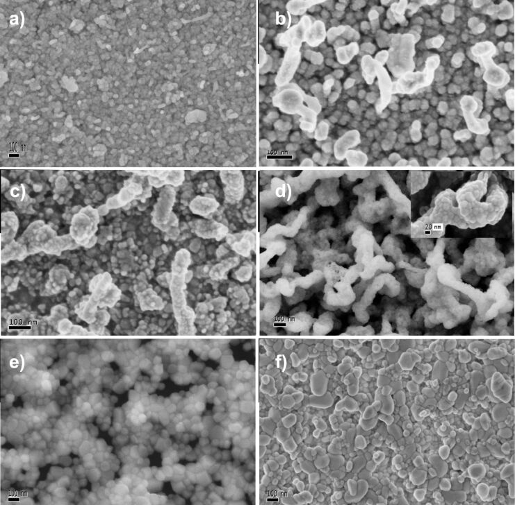
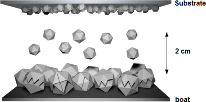
This work presents a novel technique to deposit ZnO thin films through a metal vacuum evaporation technique using colloidal nanoparticles (average size of 30 nm), which were synthesized by our research group, as source. These thin films had a thickness between 45 and 123 nm as measured by profilometry. XRD patterns of the deposited thin films were obtained. According to the HRSEM micrographs worm-shaped nanostructures are observed in samples annealed at 600 °C and this characteristic disappears as the annealing temperature increases. The films obtained were annealed from 25 to 1000 °C, showing a gradual increase in transmittance spectra up to 85%. The optical band gaps obtained for these films are about 3.22 eV. The PL measurement shows an emission in the red and in the violet region and there is a correlation with the annealing process.
本工作提出了一种新颖的技术,通过金属真空蒸发技术,使用由我们研究小组合成的胶体纳米颗粒(平均尺寸为30 nm)作为源来沉积ZnO薄膜。通过轮廓仪测量,这些薄膜的厚度在45至123 nm之间。获得了沉积薄膜的XRD图谱。根据高分辨率扫描电子显微镜图像,在600°C退火的样品中观察到蠕虫状纳米结构,并且随着退火温度的升高,这种特征消失。所获得的薄膜在25至1000°C下退火,其透射光谱显示出逐渐增加,最高可达85%。这些薄膜的光学带隙约为3.22 eV。PL测量显示在红色和紫色区域有发射,并且与退火过程存在相关性。