Barr M, Fahy A, Martens J, Jardine A P, Ward D J, Ellis J, Allison W, Dastoor P C
Centre for Organic Electronics, University of Newcastle, Callaghan, New South Wales 2308, Australia.
Cavendish Laboratory, University of Cambridge, Madingley Road, Cambridge CB3 0HE, UK.
Nat Commun. 2016 Jan 4;7:10189. doi: 10.1038/ncomms10189.
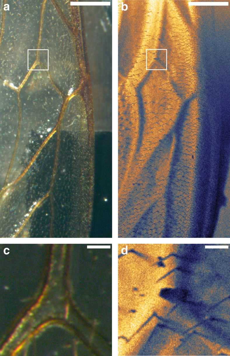
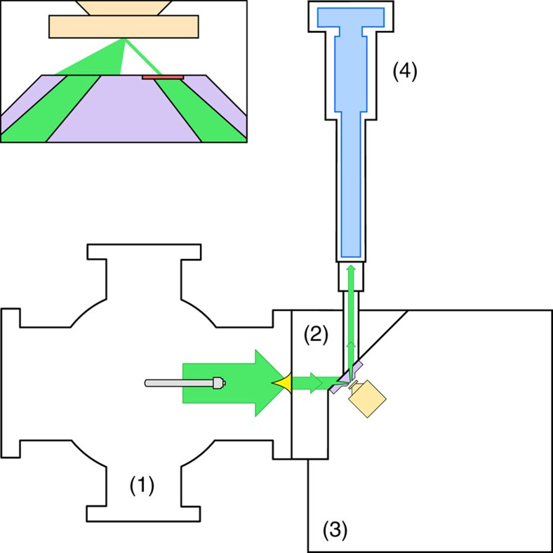
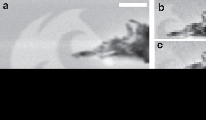
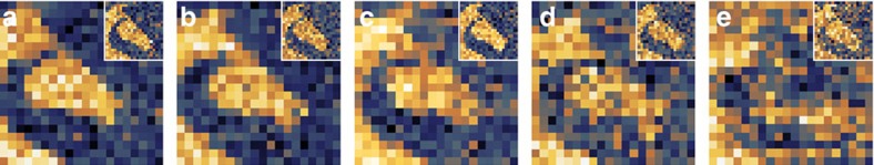
Delicate structures (such as biological samples, organic films for polymer electronics and adsorbate layers) suffer degradation under the energetic probes of traditional microscopies. Furthermore, the charged nature of these probes presents difficulties when imaging with electric or magnetic fields, or for insulating materials where the addition of a conductive coating is not desirable. Scanning helium microscopy is able to image such structures completely non-destructively by taking advantage of a neutral helium beam as a chemically, electrically and magnetically inert probe of the sample surface. Here we present scanning helium micrographs demonstrating image contrast arising from a range of mechanisms including, for the first time, chemical contrast observed from a series of metal-semiconductor interfaces. The ability of scanning helium microscopy to distinguish between materials without the risk of damage makes it ideal for investigating a wide range of systems.
精细结构(如生物样本、用于聚合物电子学的有机薄膜和吸附层)在传统显微镜的高能探针下会发生降解。此外,这些探针的带电性质在利用电场或磁场成像时,或者对于不希望添加导电涂层的绝缘材料成像时会带来困难。扫描氦显微镜能够通过利用中性氦束作为对样品表面化学、电和磁惰性的探针,对这类结构进行完全无损成像。在此,我们展示扫描氦显微镜图像,这些图像展示了由一系列机制产生的图像对比度,首次包括从一系列金属 - 半导体界面观察到的化学对比度。扫描氦显微镜能够在不造成损伤风险的情况下区分材料,这使其成为研究广泛系统的理想工具。