• 文献检索
  • 文档翻译
  • 深度研究
  • 学术资讯
  • Suppr Zotero 插件Zotero 插件
  • 邀请有礼
  • 套餐&价格
  • 历史记录
应用&插件
Suppr Zotero 插件Zotero 插件浏览器插件Mac 客户端Windows 客户端微信小程序
定价
高级版会员购买积分包购买API积分包
服务
文献检索文档翻译深度研究API 文档MCP 服务
关于我们
关于 Suppr公司介绍联系我们用户协议隐私条款
关注我们

Suppr 超能文献

核心技术专利:CN118964589B侵权必究
粤ICP备2023148730 号-1Suppr @ 2026

文献检索

告别复杂PubMed语法,用中文像聊天一样搜索,搜遍4000万医学文献。AI智能推荐,让科研检索更轻松。

立即免费搜索

文件翻译

保留排版,准确专业,支持PDF/Word/PPT等文件格式,支持 12+语言互译。

免费翻译文档

深度研究

AI帮你快速写综述,25分钟生成高质量综述,智能提取关键信息,辅助科研写作。

立即免费体验

一种用于制造纳米光子器件的可编程纳米复制成型技术。

A programmable nanoreplica molding for the fabrication of nanophotonic devices.

作者信息

Liu Longju, Zhang Jingxiang, Badshah Mohsin Ali, Dong Liang, Li Jingjing, Kim Seok-min, Lu Meng

机构信息

Department of Electrical and Computer Engineering, Iowa State University, Ames, Iowa 50011, USA.

School of Mechanical Engineering, Chung-Ang University, Seoul 156-756, Republic of Korea.

出版信息

Sci Rep. 2016 Mar 1;6:22445. doi: 10.1038/srep22445.

DOI:10.1038/srep22445
PMID:26925828
原文链接:https://pmc.ncbi.nlm.nih.gov/articles/PMC4772005/
Abstract

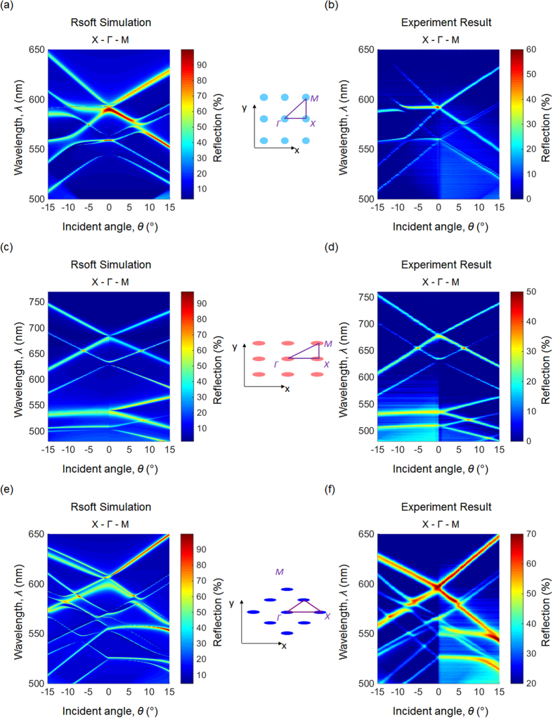
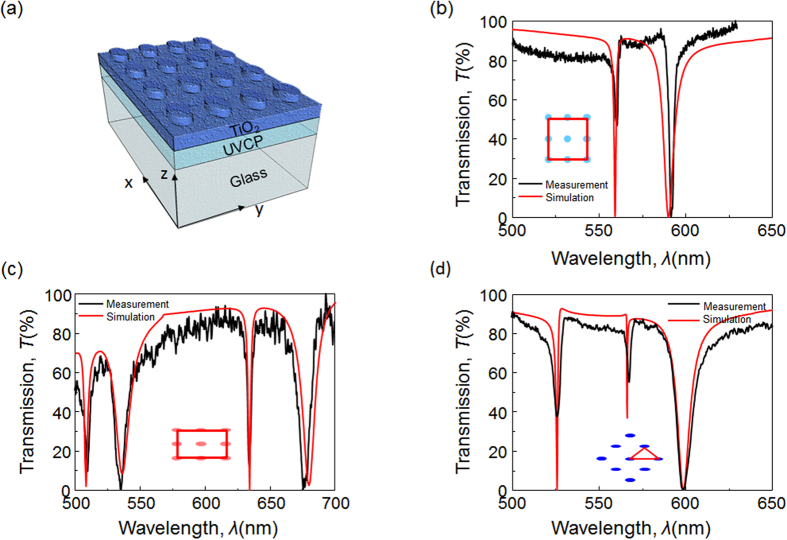
The ability to fabricate periodic structures with sub-wavelength features has a great potential for impact on integrated optics, optical sensors, and photovoltaic devices. Here, we report a programmable nanoreplica molding process to fabricate a variety of sub-micrometer periodic patterns using a single mold. The process utilizes a stretchable mold to produce the desired periodic structure in a photopolymer on glass or plastic substrates. During the replica molding process, a uniaxial force is applied to the mold and results in changes of the periodic structure, which resides on the surface of the mold. Direction and magnitude of the force determine the array geometry, including the lattice constant and arrangement. By stretching the mold, 2D arrays with square, rectangular, and triangular lattice structures can be fabricated. As one example, we present a plasmonic crystal device with surface plasmon resonances determined by the force applied during molding. In addition, photonic crystal slabs with different array patterns are fabricated and characterized. This unique process offers the capability of generating various periodic nanostructures rapidly and inexpensively.

摘要

制造具有亚波长特征的周期性结构的能力在集成光学、光学传感器和光伏器件方面具有巨大的潜在影响。在此,我们报告一种可编程的纳米复制成型工艺,该工艺使用单个模具制造各种亚微米级周期性图案。该工艺利用可拉伸模具在玻璃或塑料基板上的光聚合物中产生所需的周期性结构。在复制成型过程中,单轴力施加到模具上并导致位于模具表面的周期性结构发生变化。力的方向和大小决定了阵列几何形状,包括晶格常数和排列方式。通过拉伸模具,可以制造具有正方形、矩形和三角形晶格结构的二维阵列。作为一个例子,我们展示了一种等离子体晶体器件,其表面等离子体共振由成型过程中施加的力决定。此外,还制造并表征了具有不同阵列图案的光子晶体平板。这种独特的工艺能够快速且廉价地生成各种周期性纳米结构。

https://cdn.ncbi.nlm.nih.gov/pmc/blobs/a607/4772005/cd5fc83a8bb9/srep22445-f6.jpg
https://cdn.ncbi.nlm.nih.gov/pmc/blobs/a607/4772005/019ea943ad2d/srep22445-f1.jpg
https://cdn.ncbi.nlm.nih.gov/pmc/blobs/a607/4772005/338a2f1f288e/srep22445-f2.jpg
https://cdn.ncbi.nlm.nih.gov/pmc/blobs/a607/4772005/36ffb82b0c69/srep22445-f3.jpg
https://cdn.ncbi.nlm.nih.gov/pmc/blobs/a607/4772005/1e11866225b9/srep22445-f4.jpg
https://cdn.ncbi.nlm.nih.gov/pmc/blobs/a607/4772005/a9d123b5ecf7/srep22445-f5.jpg
https://cdn.ncbi.nlm.nih.gov/pmc/blobs/a607/4772005/cd5fc83a8bb9/srep22445-f6.jpg

相似文献

1
A programmable nanoreplica molding for the fabrication of nanophotonic devices.一种用于制造纳米光子器件的可编程纳米复制成型技术。
Sci Rep. 2016 Mar 1;6:22445. doi: 10.1038/srep22445.
2
Integrated 2D photonic crystal stack filter fabricated using nanoreplica molding.采用纳米复制成型法制造的集成二维光子晶体叠层滤波器。
Opt Express. 2010 May 24;18(11):11846-58. doi: 10.1364/OE.18.011846.
3
A strain-tunable nanoimprint lithography for linear variable photonic crystal filters.一种应变可调谐纳米压印光刻技术用于线性可变光子晶体滤波器。
Nanotechnology. 2016 Jul 22;27(29):295301. doi: 10.1088/0957-4484/27/29/295301. Epub 2016 Jun 8.
4
Multi-resonant plasmonic nanodome arrays for label-free biosensing applications.多共振等离子体纳米穹顶阵列用于无标记生物传感应用。
Nanoscale. 2013 Sep 7;5(17):8138-45. doi: 10.1039/c3nr02374e.
5
Microlens Fabrication by Replica Molding of Electro-Hydrodynamic Printing Liquid Mold.通过电流体动力打印液体模具的复制成型制造微透镜。
Micromachines (Basel). 2020 Feb 3;11(2):161. doi: 10.3390/mi11020161.
6
Fabrication and replication of arrays of single- or multicomponent nanostructures by replica molding and mechanical sectioning.通过复制成型和机械切割制造和复制单组分或多组分纳米结构阵列。
ACS Nano. 2010 Jul 27;4(7):4017-26. doi: 10.1021/nn100993t.
7
A Comprehensive Review of Micro/Nano Precision Glass Molding Molds and Their Fabrication Methods.微纳精密玻璃成型模具及其制造方法的综合综述
Micromachines (Basel). 2021 Jul 12;12(7):812. doi: 10.3390/mi12070812.
8
A stretch-tunable plasmonic structure with a polarization-dependent response.一种具有偏振依赖响应的拉伸可调谐等离子体结构。
Opt Express. 2012 Feb 27;20(5):5237-42. doi: 10.1364/OE.20.005237.
9
From molecular design and materials construction to organic nanophotonic devices.从分子设计和材料构建到有机纳米光子器件。
Acc Chem Res. 2014 Dec 16;47(12):3448-58. doi: 10.1021/ar500192v. Epub 2014 Oct 24.
10
Surface-enhanced Raman nanodomes.表面增强拉曼纳米穹顶。
Nanotechnology. 2010 Oct 15;21(41):415301. doi: 10.1088/0957-4484/21/41/415301. Epub 2010 Sep 13.

引用本文的文献

1
Recent Developments in Plasmonic Nanostructures for Metal Enhanced Fluorescence-Based Biosensing.用于基于金属增强荧光的生物传感的等离子体纳米结构的最新进展
Nanomaterials (Basel). 2020 Sep 3;10(9):1749. doi: 10.3390/nano10091749.
2
A Magnetically Controlled Soft Microrobot Steering a Guidewire in a Three-Dimensional Phantom Vascular Network.磁控软微机器人在三维虚拟血管网络中引导导丝。
Soft Robot. 2019 Feb;6(1):54-68. doi: 10.1089/soro.2018.0019. Epub 2018 Oct 12.

本文引用的文献

1
Nanostructure arrays in free-space: optical properties and applications.自由空间中的纳米结构阵列:光学性质与应用。
Rep Prog Phys. 2014 Dec;77(12):126402. doi: 10.1088/0034-4885/77/12/126402. Epub 2014 Nov 26.
2
Sculpting narrowband Fano resonances inherent in the large-area mid-infrared photonic crystal microresonators for spectroscopic imaging.塑造大面积中红外光子晶体微谐振器中固有的窄带法诺共振用于光谱成像。
Opt Express. 2014 Jul 28;22(15):18142-58. doi: 10.1364/OE.22.018142.
3
A review of roll-to-roll nanoimprint lithography.
卷对卷纳米压印光刻综述。
Nanoscale Res Lett. 2014 Jun 25;9(1):320. doi: 10.1186/1556-276X-9-320. eCollection 2014.
4
Diamond photonic crystal slab: leaky modes and modified photoluminescence emission of surface-deposited quantum dots.金刚石光子晶体平板:表面沉积量子点的泄漏模式和光致发光发射的修正。
Sci Rep. 2012;2:914. doi: 10.1038/srep00914. Epub 2012 Dec 3.
5
Photonic crystal enhanced fluorescence using a quartz substrate to reduce limits of detection.使用石英衬底的光子晶体增强荧光以降低检测限。
Opt Express. 2010 Nov 22;18(24):24793-808. doi: 10.1364/OE.18.024793.
6
Programmable soft lithography: solvent-assisted nanoscale embossing.可编程软光刻:溶剂辅助的纳米压印。
Nano Lett. 2011 Feb 9;11(2):311-5. doi: 10.1021/nl102206x. Epub 2010 Aug 5.
7
Large-area roll-to-roll and roll-to-plate nanoimprint lithography: a step toward high-throughput application of continuous nanoimprinting.大面积卷对卷和卷对板纳米压印光刻技术:迈向连续纳米压印高通量应用的一步。
ACS Nano. 2009 Aug 25;3(8):2304-10. doi: 10.1021/nn9003633.
8
Widely tunable guided-mode resonance nanoelectromechanical RGB pixels.宽可调谐导模共振纳米机电RGB像素。
Opt Express. 2007 Aug 20;15(17):10903-10. doi: 10.1364/oe.15.010903.
9
Surface plasmon generation and light transmission by isolated nanoholes and arrays of nanoholes in thin metal films.薄金属膜中孤立纳米孔和纳米孔阵列产生表面等离子体及光传输
Opt Express. 2005 Apr 18;13(8):3150-65. doi: 10.1364/opex.13.003150.