• 文献检索
  • 文档翻译
  • 深度研究
  • 学术资讯
  • Suppr Zotero 插件Zotero 插件
  • 邀请有礼
  • 套餐&价格
  • 历史记录
应用&插件
Suppr Zotero 插件Zotero 插件浏览器插件Mac 客户端Windows 客户端微信小程序
定价
高级版会员购买积分包购买API积分包
服务
文献检索文档翻译深度研究API 文档MCP 服务
关于我们
关于 Suppr公司介绍联系我们用户协议隐私条款
关注我们

Suppr 超能文献

核心技术专利:CN118964589B侵权必究
粤ICP备2023148730 号-1Suppr @ 2026

文献检索

告别复杂PubMed语法,用中文像聊天一样搜索,搜遍4000万医学文献。AI智能推荐,让科研检索更轻松。

立即免费搜索

文件翻译

保留排版,准确专业,支持PDF/Word/PPT等文件格式,支持 12+语言互译。

免费翻译文档

深度研究

AI帮你快速写综述,25分钟生成高质量综述,智能提取关键信息,辅助科研写作。

立即免费体验

大面积物理气相沉积单层和双层二硫化钼的光敏性。

Photo-sensitivity of large area physical vapor deposited mono and bilayer MoS.

作者信息

Wang Baoming, Muratore Christopher, Voevodin Andrey A, Haque Md Amanul

机构信息

Mechanical & Nuclear Engineering, the Pennsylvania State University, University Park, PA 16802 USA.

Chemical & Materials Engineering, University of Dayton, Dayton, OH 45469 USA.

出版信息

Nano Converg. 2014;1(1):22. doi: 10.1186/s40580-014-0022-6. Epub 2014 Aug 9.

DOI:10.1186/s40580-014-0022-6
PMID:28191402
原文链接:https://pmc.ncbi.nlm.nih.gov/articles/PMC5270997/
Abstract

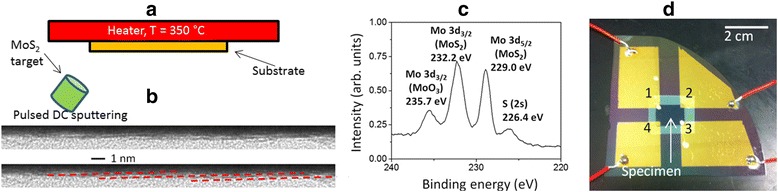
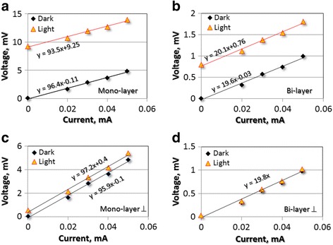
We present photosensitivity in large area physical vapour deposited mono and bi-layer MoS films. Photo-voltaic effect was observed in single layer MoS without any apparent rectifying junctions, making device fabrication straightforward. For bi-layers, no such effect was present, suggesting strong size effect in light-matter interaction. The photo-voltaic effect was observed to highly direction dependent in the film plane, which suggests that the oblique deposition configuration plays a key role in developing the rectifying potential gradient. To the best of our knowledge, this is the first report of any large area and transfer free MoS photo device with performance comparable to their exfoliated counterparts.

摘要

我们展示了大面积物理气相沉积的单层和双层MoS薄膜中的光敏性。在没有任何明显整流结的单层MoS中观察到了光伏效应,这使得器件制造变得简单直接。对于双层膜,不存在这种效应,这表明在光与物质相互作用中存在强烈的尺寸效应。观察到光伏效应在薄膜平面内高度依赖于方向,这表明倾斜沉积配置在形成整流电位梯度中起着关键作用。据我们所知,这是第一篇关于任何大面积且无需转移的MoS光电器件的报告,其性能与通过剥离法制备的同类器件相当。

https://cdn.ncbi.nlm.nih.gov/pmc/blobs/2c49/5270997/25c8a46a931f/40580_2014_22_Fig2_HTML.jpg
https://cdn.ncbi.nlm.nih.gov/pmc/blobs/2c49/5270997/233e514a206d/40580_2014_22_Fig1_HTML.jpg
https://cdn.ncbi.nlm.nih.gov/pmc/blobs/2c49/5270997/25c8a46a931f/40580_2014_22_Fig2_HTML.jpg
https://cdn.ncbi.nlm.nih.gov/pmc/blobs/2c49/5270997/233e514a206d/40580_2014_22_Fig1_HTML.jpg
https://cdn.ncbi.nlm.nih.gov/pmc/blobs/2c49/5270997/25c8a46a931f/40580_2014_22_Fig2_HTML.jpg

相似文献

1
Photo-sensitivity of large area physical vapor deposited mono and bilayer MoS.大面积物理气相沉积单层和双层二硫化钼的光敏性。
Nano Converg. 2014;1(1):22. doi: 10.1186/s40580-014-0022-6. Epub 2014 Aug 9.
2
Tailored Langmuir-Schaefer Deposition of Few-Layer MoS Nanosheet Films for Electronic Applications.用于电子应用的少层二硫化钼纳米片薄膜的定制朗缪尔-谢弗沉积法
Langmuir. 2019 Jul 30;35(30):9802-9808. doi: 10.1021/acs.langmuir.9b01000. Epub 2019 Jul 18.
3
Growth, structure and stability of sputter-deposited MoS thin films.溅射沉积MoS薄膜的生长、结构与稳定性。
Beilstein J Nanotechnol. 2017 May 22;8:1115-1126. doi: 10.3762/bjnano.8.113. eCollection 2017.
4
Large-Area Growth of Uniform Single-Layer MoS2 Thin Films by Chemical Vapor Deposition.通过化学气相沉积法大面积生长均匀单层二硫化钼薄膜
Nanoscale Res Lett. 2015 Dec;10(1):388. doi: 10.1186/s11671-015-1094-x. Epub 2015 Oct 6.
5
One-step chemically vapor deposited hybrid 1T-MoS/2H-MoS heterostructures towards methylene blue photodegradation.一步化学气相沉积法制备用于亚甲基蓝光降解的混合1T-MoS/2H-MoS异质结构
Ultrason Sonochem. 2023 May;95:106381. doi: 10.1016/j.ultsonch.2023.106381. Epub 2023 Mar 24.
6
Effect of Ultraviolet-Ozone Treatment on MoS Monolayers: Comparison of Chemical-Vapor-Deposited Polycrystalline Thin Films and Mechanically Exfoliated Single Crystal Flakes.紫外臭氧处理对二硫化钼单层的影响:化学气相沉积多晶薄膜与机械剥离单晶薄片的比较
Nanoscale Res Lett. 2019 Aug 15;14(1):278. doi: 10.1186/s11671-019-3119-3.
7
Layer-controlled CVD growth of large-area two-dimensional MoS2 films.大面积二维MoS2薄膜的层控化学气相沉积生长
Nanoscale. 2015 Feb 7;7(5):1688-95. doi: 10.1039/c4nr04532g.
8
Photoelectron spectroscopic imaging and device applications of large-area patternable single-layer MoS2 synthesized by chemical vapor deposition.化学气相沉积法合成大面积可图案化单层 MoS2 的光电子谱学成像及器件应用。
ACS Nano. 2014 May 27;8(5):4961-8. doi: 10.1021/nn501019g. Epub 2014 Apr 16.
9
Large-area, continuous and high electrical performances of bilayer to few layers MoS2 fabricated by RF sputtering via post-deposition annealing method.通过射频溅射后沉积退火法制备的双层至几层二硫化钼的大面积、连续且高电性能。
Sci Rep. 2016 Aug 5;6:30791. doi: 10.1038/srep30791.
10
Field-Effect Transistor Based on 2D Microcrystalline MoS Film Grown by Sulfurization of Atomically Layer Deposited MoO.基于原子层沉积的MoO硫化生长的二维微晶MoS薄膜的场效应晶体管
Nanomaterials (Basel). 2022 Sep 20;12(19):3262. doi: 10.3390/nano12193262.

引用本文的文献

1
Microscopic evidence of strong interactions between chemical vapor deposited 2D MoS film and SiO growth template.化学气相沉积二维MoS薄膜与SiO生长模板之间强相互作用的微观证据。
Nano Converg. 2021 Apr 9;8(1):11. doi: 10.1186/s40580-021-00262-x.
2
Improved optical performance of multi-layer MoS phototransistor with see-through metal electrode.具有透明金属电极的多层MoS光晶体管的光学性能改善
Nano Converg. 2019 Oct 2;6(1):32. doi: 10.1186/s40580-019-0202-5.
3
Tunable Wetting Property in Growth Mode-Controlled WS Thin Films.生长模式可控的WS薄膜中的可调润湿性

本文引用的文献

1
Thermal anisotropy in nano-crystalline MoS2 thin films.纳米晶 MoS2 薄膜的热各向异性。
Phys Chem Chem Phys. 2014 Jan 21;16(3):1008-14. doi: 10.1039/c3cp53746c. Epub 2013 Nov 27.
2
Orientation dependent thermal conductance in single-layer MoS2.单层 MoS2 中依赖于取向的热导
Sci Rep. 2013;3:2209. doi: 10.1038/srep02209.
3
Extraordinary sunlight absorption and one nanometer thick photovoltaics using two-dimensional monolayer materials.使用二维单层材料实现非凡的太阳光吸收和一纳米厚的光伏器件。
Nanoscale Res Lett. 2017 Dec;12(1):262. doi: 10.1186/s11671-017-2030-z. Epub 2017 Apr 7.
Nano Lett. 2013 Aug 14;13(8):3664-70. doi: 10.1021/nl401544y. Epub 2013 Jul 10.
4
Ultrasensitive photodetectors based on monolayer MoS2.基于单层 MoS2 的超高灵敏度光电探测器。
Nat Nanotechnol. 2013 Jul;8(7):497-501. doi: 10.1038/nnano.2013.100. Epub 2013 Jun 9.
5
Strong light-matter interactions in heterostructures of atomically thin films.原子层薄膜异质结构中的强光物质相互作用。
Science. 2013 Jun 14;340(6138):1311-4. doi: 10.1126/science.1235547. Epub 2013 May 2.
6
Electron-hole transport and photovoltaic effect in gated MoS2 Schottky junctions.门控二硫化钼肖特基结中的电子-空穴输运与光伏效应。
Sci Rep. 2013;3:1634. doi: 10.1038/srep01634.
7
Large and tunable photothermoelectric effect in single-layer MoS2.单层 MoS2 中的大可调光热电效应。
Nano Lett. 2013 Feb 13;13(2):358-63. doi: 10.1021/nl303321g. Epub 2013 Jan 11.
8
High performance multilayer MoS2 transistors with scandium contacts.具有钪接触的高性能多层 MoS2 晶体管。
Nano Lett. 2013 Jan 9;13(1):100-5. doi: 10.1021/nl303583v. Epub 2012 Dec 19.
9
Electronics and optoelectronics of two-dimensional transition metal dichalcogenides.二维过渡金属二卤族化合物的电子学和光电学。
Nat Nanotechnol. 2012 Nov;7(11):699-712. doi: 10.1038/nnano.2012.193.
10
Layered semiconductor molybdenum disulfide nanomembrane based Schottky-barrier solar cells.基于层状半导体二硫化钼纳米膜的肖特基势垒太阳能电池。
Nanoscale. 2012 Dec 7;4(23):7399-405. doi: 10.1039/c2nr32394j.