Baek Seung Hyun, Choi Yura, Choi Woong
School of Advanced Materials Engineering, Kookmin University, Seoul, 02707, South Korea.
Nanoscale Res Lett. 2015 Dec;10(1):388. doi: 10.1186/s11671-015-1094-x. Epub 2015 Oct 6.
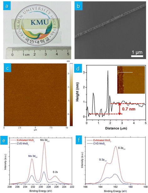
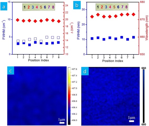
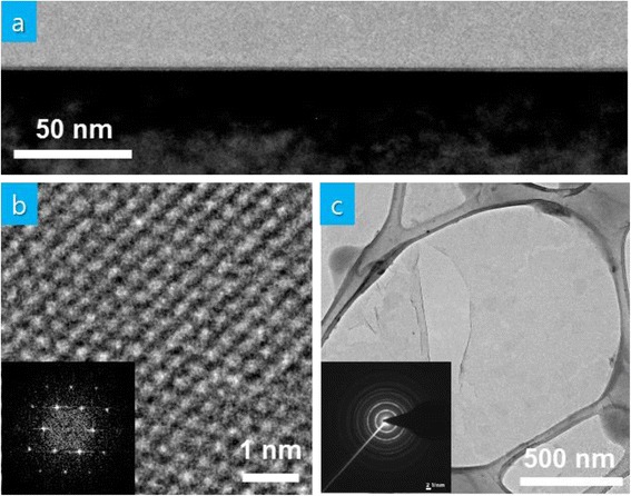
We report the largest-size thin films of uniform single-layer MoS2 on sapphire substrates grown by chemical vapor deposition based on the reaction of gaseous MoO3 and S evaporated from solid sources. The as-grown thin films of single-layer MoS2 were continuous and uniform in thickness for more than 4 cm without the existence of triangular-shaped MoS2 clusters. Compared to mechanically exfoliated crystals, the as-grown single-layer MoS2 thin films possessed consistent chemical valence states and crystal structure along with strong photoluminescence emission and optical absorbance at high energy. These results demonstrate that it is possible to scale up the growth of uniform single-layer MoS2 thin films, providing potentially important implications on realizing high-performance MoS2 devices.
我们报道了基于气态MoO₃与从固态源蒸发的S之间的反应,通过化学气相沉积法在蓝宝石衬底上生长出的最大尺寸的均匀单层MoS₂薄膜。所生长的单层MoS₂薄膜连续且厚度均匀,超过4厘米,不存在三角形的MoS₂簇。与机械剥离的晶体相比,所生长的单层MoS₂薄膜具有一致的化学价态和晶体结构,同时在高能下具有强烈的光致发光发射和光吸收。这些结果表明,扩大均匀单层MoS₂薄膜的生长是可能的,这对实现高性能MoS₂器件具有潜在的重要意义。