• 文献检索
  • 文档翻译
  • 深度研究
  • 学术资讯
  • Suppr Zotero 插件Zotero 插件
  • 邀请有礼
  • 套餐&价格
  • 历史记录
应用&插件
Suppr Zotero 插件Zotero 插件浏览器插件Mac 客户端Windows 客户端微信小程序
定价
高级版会员购买积分包购买API积分包
服务
文献检索文档翻译深度研究API 文档MCP 服务
关于我们
关于 Suppr公司介绍联系我们用户协议隐私条款
关注我们

Suppr 超能文献

核心技术专利:CN118964589B侵权必究
粤ICP备2023148730 号-1Suppr @ 2026

文献检索

告别复杂PubMed语法,用中文像聊天一样搜索,搜遍4000万医学文献。AI智能推荐,让科研检索更轻松。

立即免费搜索

文件翻译

保留排版,准确专业,支持PDF/Word/PPT等文件格式,支持 12+语言互译。

免费翻译文档

深度研究

AI帮你快速写综述,25分钟生成高质量综述,智能提取关键信息,辅助科研写作。

立即免费体验

Area-Selective Atomic Layer Deposition of InO:H Using a μ-Plasma Printer for Local Area Activation.

作者信息

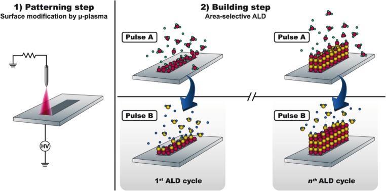
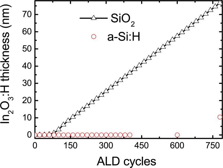
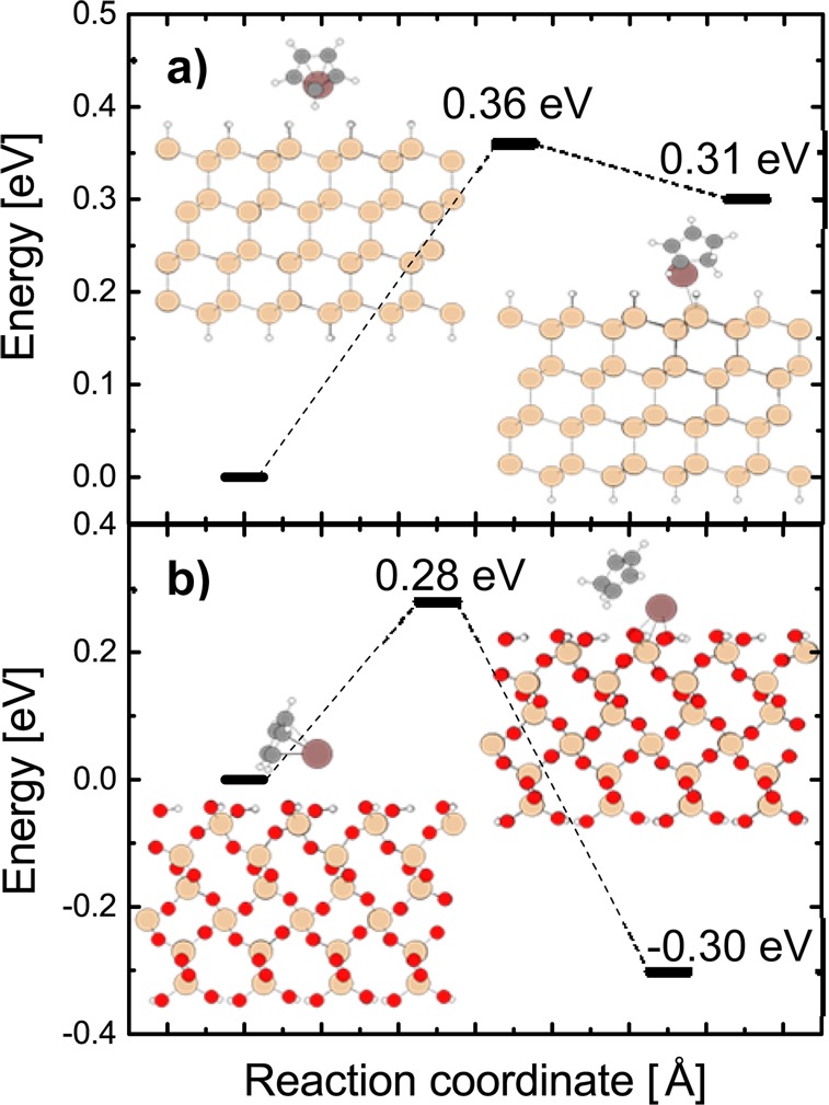
Mameli Alfredo, Kuang Yinghuan, Aghaee Morteza, Ande Chaitanya K, Karasulu Bora, Creatore Mariadriana, Mackus Adriaan J M, Kessels Wilhelmus M M, Roozeboom Fred

机构信息

Department of Applied Physics, Eindhoven University of Technology , PO Box 513, 5600 MB Eindhoven, The Netherlands.

Department of Applied Physics, Eindhoven University of Technology, PO Box 513, 5600 MB Eindhoven, The Netherlands; Department Thin Film Technology, TNO, High Tech Campus 21, 5656 AE Eindhoven, The Netherlands.

出版信息

Chem Mater. 2017 Feb 14;29(3):921-925. doi: 10.1021/acs.chemmater.6b04469. Epub 2017 Jan 23.

DOI:10.1021/acs.chemmater.6b04469
PMID:28405058
原文链接:https://pmc.ncbi.nlm.nih.gov/articles/PMC5384477/
Abstract
摘要
https://cdn.ncbi.nlm.nih.gov/pmc/blobs/8387/5384477/2a718ae35db1/cm-2016-044697_0006.jpg
https://cdn.ncbi.nlm.nih.gov/pmc/blobs/8387/5384477/e1e172f7cb55/cm-2016-044697_0001.jpg
https://cdn.ncbi.nlm.nih.gov/pmc/blobs/8387/5384477/baa419f737a7/cm-2016-044697_0002.jpg
https://cdn.ncbi.nlm.nih.gov/pmc/blobs/8387/5384477/ab8e5faea15c/cm-2016-044697_0003.jpg
https://cdn.ncbi.nlm.nih.gov/pmc/blobs/8387/5384477/6ab165410351/cm-2016-044697_0004.jpg
https://cdn.ncbi.nlm.nih.gov/pmc/blobs/8387/5384477/17cd3585f2a5/cm-2016-044697_0005.jpg
https://cdn.ncbi.nlm.nih.gov/pmc/blobs/8387/5384477/2a718ae35db1/cm-2016-044697_0006.jpg

相似文献

1
Area-Selective Atomic Layer Deposition of InO:H Using a μ-Plasma Printer for Local Area Activation.使用μ-等离子体打印机进行局部区域活化的InO:H区域选择性原子层沉积
Chem Mater. 2017 Feb 14;29(3):921-925. doi: 10.1021/acs.chemmater.6b04469. Epub 2017 Jan 23.
2
Electron Scattering and Doping Mechanisms in Solid-Phase-Crystallized In2O3:H Prepared by Atomic Layer Deposition.原子层沉积法制备固相结晶 In2O3:H 中的电子散射和掺杂机制。
ACS Appl Mater Interfaces. 2015 Aug 5;7(30):16723-9. doi: 10.1021/acsami.5b04420. Epub 2015 Jul 23.
3
Low-Temperature Growth of Indium Oxide Thin Film by Plasma-Enhanced Atomic Layer Deposition Using Liquid Dimethyl(N-ethoxy-2,2-dimethylpropanamido)indium for High-Mobility Thin Film Transistor Application.采用液体二甲基(N-乙氧基-2,2-二甲基丙酰胺基)铟通过等离子体增强原子层沉积低温生长氧化铟薄膜在高迁移率薄膜晶体管中的应用。
ACS Appl Mater Interfaces. 2016 Oct 12;8(40):26924-26931. doi: 10.1021/acsami.6b07332. Epub 2016 Sep 27.
4
High-Performance On-Chip Supercapacitors Based on Mesoporous Silicon Coated with Ultrathin Atomic Layer-Deposited InO Films.基于涂覆有超薄原子层沉积InO薄膜的介孔硅的高性能片上超级电容器。
ACS Appl Mater Interfaces. 2019 Jan 9;11(1):747-752. doi: 10.1021/acsami.8b17093. Epub 2018 Dec 21.
5
Indium-tris-guanidinates: a promising class of precursors for water assisted atomic layer deposition of In2O3 thin films.铟三胍盐:水辅助原子层沉积法制备 In2O3 薄膜的有前景的前体材料。
Dalton Trans. 2014 Jan 21;43(3):937-40. doi: 10.1039/c3dt52746h. Epub 2013 Nov 22.
6
Flexible and High-Performance Amorphous Indium Zinc Oxide Thin-Film Transistor Using Low-Temperature Atomic Layer Deposition.使用低温原子层沉积技术的灵活且高性能非晶态氧化铟锌薄膜晶体管。
ACS Appl Mater Interfaces. 2016 Dec 14;8(49):33821-33828. doi: 10.1021/acsami.6b11774. Epub 2016 Nov 30.
7
Atomic Layer Deposition of InO:H from InCp and HO/O: Microstructure and Isotope Labeling Studies.InO:H 的原子层沉积来自 InCp 和 HO/O: 微结构和同位素标记研究。
ACS Appl Mater Interfaces. 2017 Jan 11;9(1):592-601. doi: 10.1021/acsami.6b13560. Epub 2016 Dec 27.
8
Local Structure and Point-Defect-Dependent Area-Selective Atomic Layer Deposition Approach for Facile Synthesis of p-CuO/n-ZnO Segmented Nanojunctions.用于简便合成 p-CuO/n-ZnO 分段纳米结的局部结构和点缺陷依赖性区域选择性原子层沉积方法。
ACS Appl Mater Interfaces. 2018 Oct 31;10(43):37671-37678. doi: 10.1021/acsami.8b12584. Epub 2018 Oct 16.
9
Improving yield and performance in ZnO thin-film transistors made using selective area deposition.提高使用选择性区域沉积法制备的氧化锌薄膜晶体管的产量和性能。
ACS Appl Mater Interfaces. 2015 Feb 4;7(4):2754-9. doi: 10.1021/am5077638. Epub 2015 Jan 20.
10
Perovskite Solar Cells Based on Low-Temperature Processed Indium Oxide Electron Selective Layers.基于低温处理氧化铟电子选择层的钙钛矿太阳能电池。
ACS Appl Mater Interfaces. 2016 Apr 6;8(13):8460-6. doi: 10.1021/acsami.5b12849. Epub 2016 Mar 25.

引用本文的文献

1
Area Selective Atomic Layer Deposition for the Use on Active Implants: An Overview of Available Process Technology.用于有源植入物的区域选择性原子层沉积:可用工艺技术概述
Adv Healthc Mater. 2025 Feb;14(4):e2403149. doi: 10.1002/adhm.202403149. Epub 2024 Dec 26.
2
Atmospheric-pressure atomic layer deposition: recent applications and new emerging applications in high-porosity/3D materials.大气压原子层沉积:在高孔隙率/三维材料中的近期应用及新出现的应用
Dalton Trans. 2023 Aug 1;52(30):10254-10277. doi: 10.1039/d3dt01204b.
3
Relation between Reactive Surface Sites and Precursor Choice for Area-Selective Atomic Layer Deposition Using Small Molecule Inhibitors.

本文引用的文献

1
A Process for Topographically Selective Deposition on 3D Nanostructures by Ion Implantation.通过离子注入实现三维纳米结构的地形选择性沉积的方法。
ACS Nano. 2016 Apr 26;10(4):4451-8. doi: 10.1021/acsnano.6b00094. Epub 2016 Mar 15.
2
Electron Scattering and Doping Mechanisms in Solid-Phase-Crystallized In2O3:H Prepared by Atomic Layer Deposition.原子层沉积法制备固相结晶 In2O3:H 中的电子散射和掺杂机制。
ACS Appl Mater Interfaces. 2015 Aug 5;7(30):16723-9. doi: 10.1021/acsami.5b04420. Epub 2015 Jul 23.
3
The use of atomic layer deposition in advanced nanopatterning.
使用小分子抑制剂的区域选择性原子层沉积中反应性表面位点与前驱体选择之间的关系
J Phys Chem C Nanomater Interfaces. 2022 Mar 17;126(10):4845-4853. doi: 10.1021/acs.jpcc.1c10816. Epub 2022 Mar 8.
4
Inherently Area-Selective Atomic Layer Deposition of Manganese Oxide through Electronegativity-Induced Adsorption.通过电负性诱导吸附实现氧化锰的本征区域选择性原子层沉积
Molecules. 2021 May 20;26(10):3056. doi: 10.3390/molecules26103056.
5
From the Bottom-Up: Toward Area-Selective Atomic Layer Deposition with High Selectivity.自下而上:迈向具有高选择性的区域选择性原子层沉积
Chem Mater. 2019 Jan 8;31(1):2-12. doi: 10.1021/acs.chemmater.8b03454. Epub 2018 Dec 19.
6
Area-Selective Atomic Layer Deposition of SiO Using Acetylacetone as a Chemoselective Inhibitor in an ABC-Type Cycle.使用乙酰丙酮作为 ABC 型循环中的化学选择抑制剂进行 SiO 的区域选择性原子层沉积。
ACS Nano. 2017 Sep 26;11(9):9303-9311. doi: 10.1021/acsnano.7b04701. Epub 2017 Sep 7.
原子层沉积在先进纳米图案化中的应用。
Nanoscale. 2014 Oct 7;6(19):10941-60. doi: 10.1039/c4nr01954g.
4
Nanopatterning by direct-write atomic layer deposition.直接写入原子层沉积的纳米图案化。
Nanoscale. 2012 Aug 7;4(15):4477-80. doi: 10.1039/c2nr30664f. Epub 2012 Jul 3.
5
Activation of surface hydroxyl groups by modification of H-terminated Si(111) surfaces.通过修饰 H 终止的 Si(111)表面来激活表面羟基基团。
J Am Chem Soc. 2012 May 30;134(21):8869-74. doi: 10.1021/ja300270w. Epub 2012 May 15.
6
Electroactive microwell arrays for highly efficient single-cell trapping and analysis.用于高效单细胞捕获和分析的电活性微流控芯片阵列。
Small. 2011 Nov 18;7(22):3239-47. doi: 10.1002/smll.201101028. Epub 2011 Sep 20.
7
A consistent and accurate ab initio parametrization of density functional dispersion correction (DFT-D) for the 94 elements H-Pu.针对 H-Pu 94 个元素,进行了一致且准确的从头计算(ab initio)密度泛函色散校正(DFT-D)参数化。
J Chem Phys. 2010 Apr 21;132(15):154104. doi: 10.1063/1.3382344.
8
Surface-patterned electrode bioreactor for electrical stimulation.用于电刺激的表面图案化电极生物反应器。
Lab Chip. 2010 Mar 21;10(6):692-700. doi: 10.1039/b917743d. Epub 2010 Jan 5.
9
Nanopatterning Si(111) surfaces as a selective surface-chemistry route.纳米图案化硅(111)表面作为一种选择性的表面化学途径。
Nat Mater. 2010 Mar;9(3):266-71. doi: 10.1038/nmat2611. Epub 2010 Jan 10.
10
Efficiency enhancement of polymer solar cells by patterning nanoscale indium tin oxide layer.通过对纳米级氧化铟锡层进行图案化处理提高聚合物太阳能电池的效率
J Nanosci Nanotechnol. 2008 Oct;8(10):5279-83. doi: 10.1166/jnn.2008.1087.