• 文献检索
  • 文档翻译
  • 深度研究
  • 学术资讯
  • Suppr Zotero 插件Zotero 插件
  • 邀请有礼
  • 套餐&价格
  • 历史记录
应用&插件
Suppr Zotero 插件Zotero 插件浏览器插件Mac 客户端Windows 客户端微信小程序
定价
高级版会员购买积分包购买API积分包
服务
文献检索文档翻译深度研究API 文档MCP 服务
关于我们
关于 Suppr公司介绍联系我们用户协议隐私条款
关注我们

Suppr 超能文献

核心技术专利:CN118964589B侵权必究
粤ICP备2023148730 号-1Suppr @ 2026

文献检索

告别复杂PubMed语法,用中文像聊天一样搜索,搜遍4000万医学文献。AI智能推荐,让科研检索更轻松。

立即免费搜索

文件翻译

保留排版,准确专业,支持PDF/Word/PPT等文件格式,支持 12+语言互译。

免费翻译文档

深度研究

AI帮你快速写综述,25分钟生成高质量综述,智能提取关键信息,辅助科研写作。

立即免费体验

室温电导率超过 10 S cm 的宽带隙 BaSnO 薄膜。

Wide bandgap BaSnO films with room temperature conductivity exceeding 10 S cm.

机构信息

Chemical Engineering and Materials Science, University of Minnesota-Twin Cities, Minneapolis, Minnesota 55455, USA.

Department of Energy, Environmental, and Chemical Engineering, Washington University, St Louis, Missouri 63130, USA.

出版信息

Nat Commun. 2017 May 5;8:15167. doi: 10.1038/ncomms15167.

DOI:10.1038/ncomms15167
PMID:28474675
原文链接:https://pmc.ncbi.nlm.nih.gov/articles/PMC5424175/
Abstract

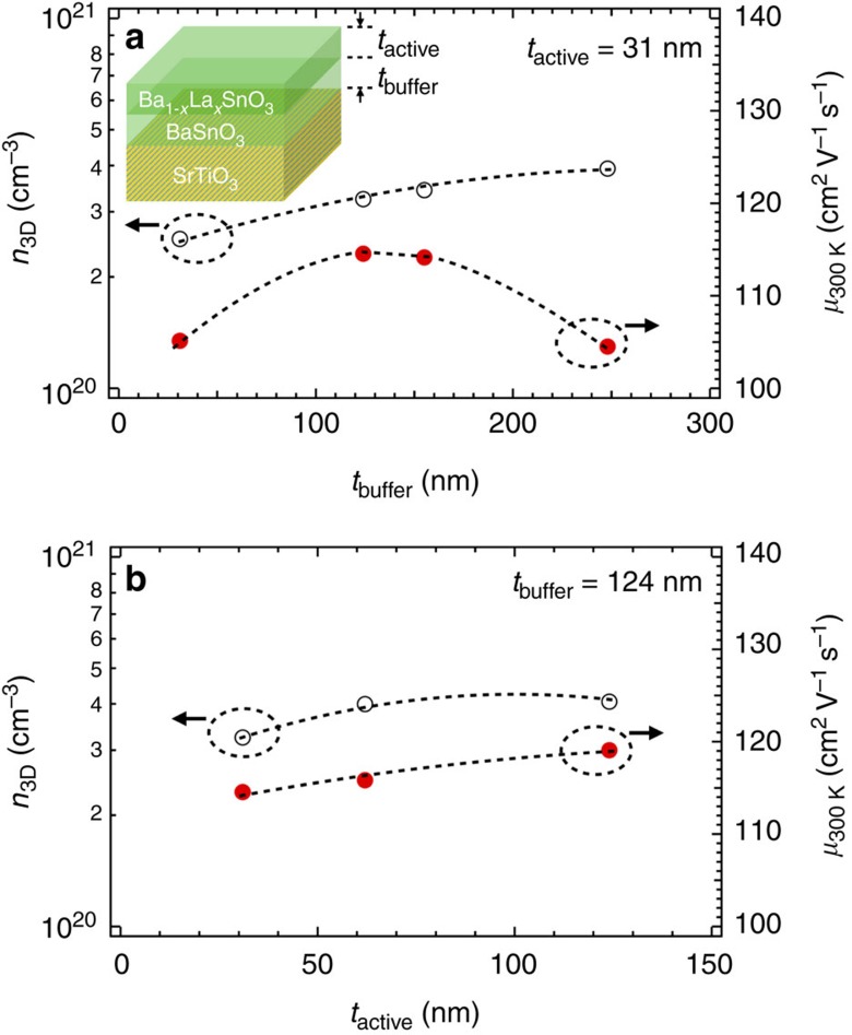
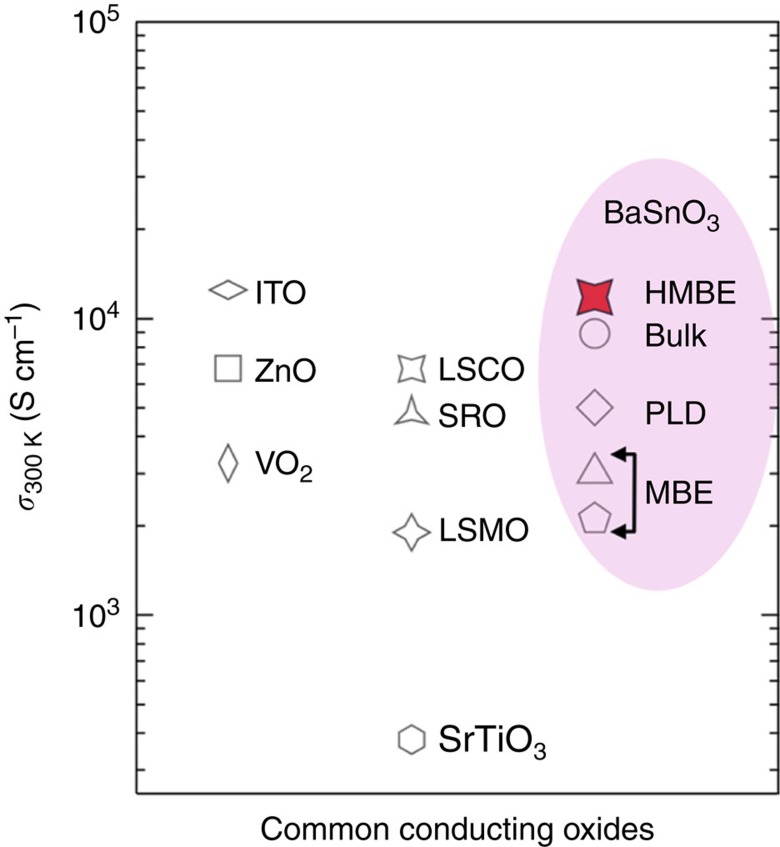
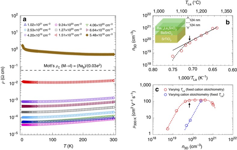
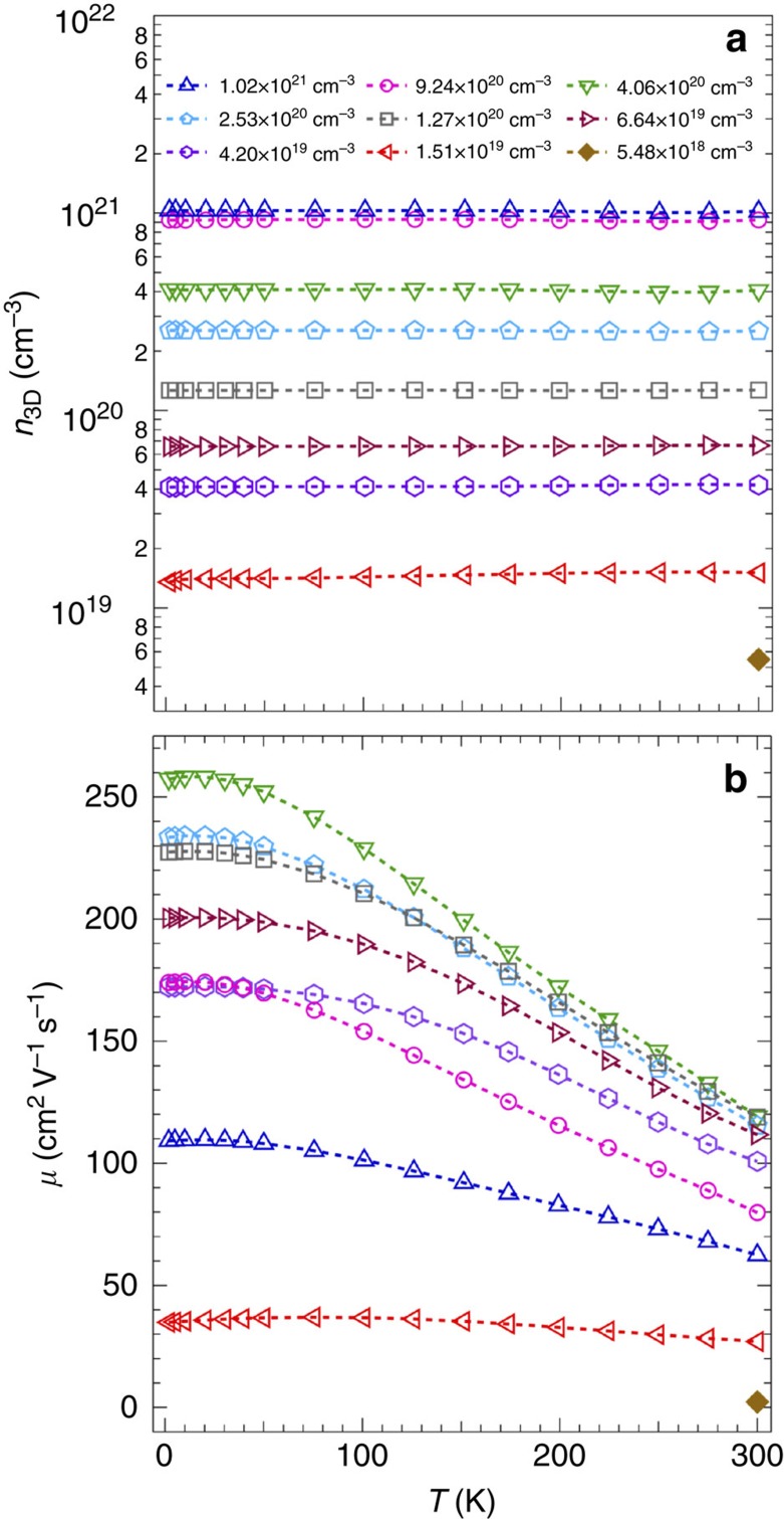
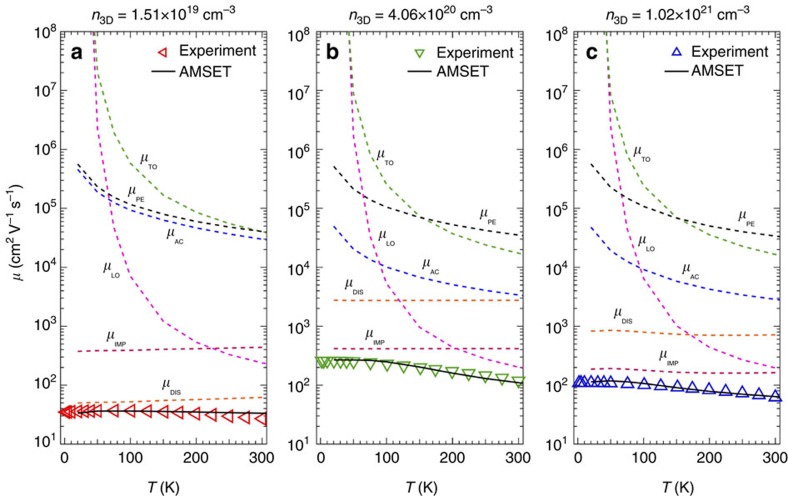
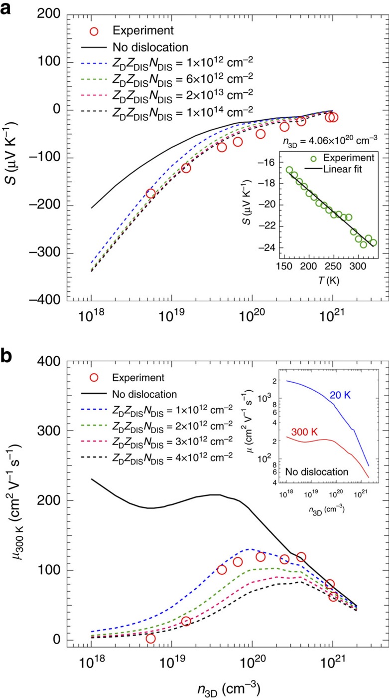
Wide bandgap perovskite oxides with high room temperature conductivities and structural compatibility with a diverse family of organic/inorganic perovskite materials are of significant interest as transparent conductors and as active components in power electronics. Such materials must also possess high room temperature mobility to minimize power consumption and to enable high-frequency applications. Here, we report n-type BaSnO films grown using hybrid molecular beam epitaxy with room temperature conductivity exceeding 10 S cm. Significantly, these films show room temperature mobilities up to 120 cm V s even at carrier concentrations above 3 × 10 cm together with a wide bandgap (3 eV). We examine the mobility-limiting scattering mechanisms by calculating temperature-dependent mobility, and Seebeck coefficient using the Boltzmann transport framework and ab-initio calculations. These results place perovskite oxide semiconductors for the first time on par with the highly successful III-N system, thereby bringing all-transparent, high-power oxide electronics operating at room temperature a step closer to reality.

摘要

宽带隙钙钛矿氧化物具有高的室温电导率和与各种有机/无机钙钛矿材料的结构兼容性,作为透明导体和在电力电子学中的有源元件具有重要意义。这些材料还必须具有高的室温迁移率,以最小化功耗并实现高频应用。在这里,我们报告了使用杂化分子束外延生长的 n 型 BaSnO 薄膜,其室温电导率超过 10 S cm。值得注意的是,这些薄膜在载流子浓度高于 3×10 cm 时,室温迁移率高达 120 cm V s ,同时具有宽的能带隙(3 eV)。我们通过使用玻尔兹曼输运框架和从头计算来计算温度相关的迁移率和 Seebeck 系数,来研究限制迁移率的散射机制。这些结果首次使钙钛矿氧化物半导体与非常成功的 III-N 系统相媲美,从而使全透明、高功率氧化物电子学在室温下的应用更接近现实。

https://cdn.ncbi.nlm.nih.gov/pmc/blobs/67fa/5424175/69dc1e9ce637/ncomms15167-f6.jpg
https://cdn.ncbi.nlm.nih.gov/pmc/blobs/67fa/5424175/983f2facc3ca/ncomms15167-f1.jpg
https://cdn.ncbi.nlm.nih.gov/pmc/blobs/67fa/5424175/81c0c4dcd59f/ncomms15167-f2.jpg
https://cdn.ncbi.nlm.nih.gov/pmc/blobs/67fa/5424175/bf906462921f/ncomms15167-f3.jpg
https://cdn.ncbi.nlm.nih.gov/pmc/blobs/67fa/5424175/305d4dacdd05/ncomms15167-f4.jpg
https://cdn.ncbi.nlm.nih.gov/pmc/blobs/67fa/5424175/ece48ab0c61d/ncomms15167-f5.jpg
https://cdn.ncbi.nlm.nih.gov/pmc/blobs/67fa/5424175/69dc1e9ce637/ncomms15167-f6.jpg

相似文献

1
Wide bandgap BaSnO films with room temperature conductivity exceeding 10 S cm.室温电导率超过 10 S cm 的宽带隙 BaSnO 薄膜。
Nat Commun. 2017 May 5;8:15167. doi: 10.1038/ncomms15167.
2
Depletion Mode MOSFET Using La-Doped BaSnO as a Channel Material.采用掺镧钡锡氧化物作为沟道材料的耗尽型 MOSFET。
ACS Appl Mater Interfaces. 2018 Jun 27;10(25):21061-21065. doi: 10.1021/acsami.8b05229. Epub 2018 Jun 18.
3
Room-Temperature-Synthesized High-Mobility Transparent Amorphous CdO-GaO Alloys with Widely Tunable Electronic Bands.室温合成的具有宽可调电子带隙的高迁移率透明非晶态 CdO-GaO 合金。
ACS Appl Mater Interfaces. 2018 Feb 28;10(8):7239-7247. doi: 10.1021/acsami.7b18254. Epub 2018 Feb 12.
4
Oxide Two-Dimensional Electron Gas with High Mobility at Room-Temperature.室温下具有高迁移率的氧化物二维电子气
Adv Sci (Weinh). 2022 Apr;9(12):e2105652. doi: 10.1002/advs.202105652. Epub 2022 Feb 20.
5
Effect of Threading Dislocations on the Electronic Structure of La-Doped BaSnO Thin Films.位错对掺镧的BaSnO薄膜电子结构的影响。
Materials (Basel). 2022 Mar 25;15(7):2417. doi: 10.3390/ma15072417.
6
High Mobility in Nanocrystal-Based Transparent Conducting Oxide Thin Films.基于纳米晶的透明导电氧化物薄膜的高迁移率。
ACS Nano. 2018 Apr 24;12(4):3200-3208. doi: 10.1021/acsnano.7b06783. Epub 2018 Mar 19.
7
Low-Temperature Postfunctionalization of Highly Conductive Oxide Thin-Films toward Solution-Based Large-Scale Electronics.低温后功能化高导电氧化物薄膜以实现基于溶液的大规模电子学。
ACS Appl Mater Interfaces. 2017 Aug 9;9(31):26191-26200. doi: 10.1021/acsami.7b07528. Epub 2017 Jul 31.
8
Plasmon-Phonon Coupling in Electrostatically Gated β-GaO Films with Mobility Exceeding 200 cm V s.迁移率超过200 cm² V⁻¹ s⁻¹的静电栅控β-GaO薄膜中的等离子体-声子耦合
ACS Nano. 2022 Jun 28;16(6):8812-8819. doi: 10.1021/acsnano.1c09535. Epub 2022 Apr 18.
9
Realization of Cu-Doped p-Type ZnO Thin Films by Molecular Beam Epitaxy.通过分子束外延实现铜掺杂的p型氧化锌薄膜
ACS Appl Mater Interfaces. 2015 Apr 29;7(16):8894-9. doi: 10.1021/acsami.5b01564. Epub 2015 Apr 14.
10
Engineering SrSnO Phases and Electron Mobility at Room Temperature Using Epitaxial Strain.利用外延应变工程 SrSnO 相和室温下的电子迁移率。
ACS Appl Mater Interfaces. 2018 Dec 19;10(50):43802-43808. doi: 10.1021/acsami.8b16592. Epub 2018 Dec 4.

引用本文的文献

1
Oxygen Deficiency Modulated La-Doped BaSnO Films Showing Improved Light Transmittance.氧缺乏调制的掺镧BaSnO薄膜具有改善的透光率。
Materials (Basel). 2025 Apr 8;18(8):1696. doi: 10.3390/ma18081696.
2
Ultralow-Resistance Contacts to Heavily Doped p-Type NbWS Thin Films Grown by Atomic Layer Deposition.通过原子层沉积生长的重掺杂p型NbWS薄膜的超低电阻接触
ACS Appl Mater Interfaces. 2025 Feb 19;17(7):10931-10941. doi: 10.1021/acsami.4c16889. Epub 2025 Feb 6.
3
Enabling 2D Electron Gas with High Room-Temperature Electron Mobility Exceeding 100 cm Vs at a Perovskite Oxide Interface.

本文引用的文献

1
Alloying ZnS in the hexagonal phase to create high-performing transparent conducting materials.在六方相中合金化硫化锌以制备高性能透明导电材料。
Phys Chem Chem Phys. 2016 Aug 10;18(32):22628-35. doi: 10.1039/c6cp01278g.
2
Direct Observation of Electrostatically Driven Band Gap Renormalization in a Degenerate Perovskite Transparent Conducting Oxide.直接观察到简并钙钛矿透明导电氧化物中静电驱动的带隙重整化。
Phys Rev Lett. 2016 Jan 15;116(2):027602. doi: 10.1103/PhysRevLett.116.027602.
3
Emergent phenomena at oxide interfaces.氧化物界面的涌现现象。
在钙钛矿氧化物界面实现具有高于100 cm²V⁻¹s⁻¹的室温电子迁移率的二维电子气。
Adv Mater. 2024 Dec;36(50):e2409076. doi: 10.1002/adma.202409076. Epub 2024 Oct 22.
4
Reconfigurable optoelectronic transistors for multimodal recognition.用于多模态识别的可重构光电子晶体管
Nat Commun. 2024 Apr 16;15(1):3257. doi: 10.1038/s41467-024-47580-2.
5
Plasma-Induced 2D Electron Transport at Hetero-Phase Titanium Oxide Interface.等离子体诱导的异相氧化钛界面二维电子输运
Adv Sci (Weinh). 2024 Feb;11(5):e2304919. doi: 10.1002/advs.202304919. Epub 2023 Dec 7.
6
La-doped BaSnO3 for electromagnetic shielding transparent conductors.用于电磁屏蔽透明导体的镧掺杂锡酸钡
Nano Converg. 2023 Oct 28;10(1):50. doi: 10.1186/s40580-023-00397-z.
7
Strong conductivity enhancement of La-doped BaSnO transparent films on AlO with the assistance of templated epitaxy for electromagnetic shielding in extreme environments.在模板外延辅助下,La掺杂的BaSnO透明薄膜在AlO上的强导电性增强,用于极端环境中的电磁屏蔽。
Nano Converg. 2023 Feb 15;10(1):9. doi: 10.1186/s40580-023-00355-9.
8
Structure Modification, Evolution, and Compositional Changes of Highly Conductive La:BaSnO Thin Films Annealed in Vacuum and Air Atmosphere.在真空和空气气氛中退火的高导电性镧掺杂钡锡氧化物薄膜的结构改性、演化及成分变化
Nanomaterials (Basel). 2022 Jul 14;12(14):2408. doi: 10.3390/nano12142408.
9
Proton Conduction in Acceptor-Doped BaSnO: The Impact of the Interaction between Ionic Defects and Acceptor Impurities.受主掺杂BaSnO中的质子传导:离子缺陷与受主杂质间相互作用的影响
Materials (Basel). 2022 Jul 8;15(14):4795. doi: 10.3390/ma15144795.
10
Strain sensitivity of band structure and electron mobility in perovskite BaSnO: first-principles calculation.钙钛矿BaSnO中能带结构和电子迁移率的应变敏感性:第一性原理计算
RSC Adv. 2019 May 7;9(25):14072-14077. doi: 10.1039/c9ra02146a.
Nat Mater. 2012 Jan 24;11(2):103-13. doi: 10.1038/nmat3223.
4
The interface is still the device.界面仍然是该设备。
Nat Mater. 2012 Jan 24;11(2):91. doi: 10.1038/nmat3244.
5
Oxide electronics: Interface takes charge over Si.氧化物电子学:界面掌控硅。
Nat Mater. 2011 Mar;10(3):168-9. doi: 10.1038/nmat2965.
6
Oxide electronics: Upward mobility rocks!氧化物电子学:向上迁移率优势尽显!
Nat Mater. 2010 Nov;9(11):881-3. doi: 10.1038/nmat2888.
7
Materials science: Enter the oxides.材料科学:走进氧化物。
Nature. 2009 May 7;459(7243):28-30. doi: 10.1038/459028a.
8
Thousandfold change in resistivity in magnetoresistive la-ca-mn-o films.磁阻 La-Ca-Mn-O 薄膜中的电阻率变化达千倍。
Science. 1994 Apr 15;264(5157):413-5. doi: 10.1126/science.264.5157.413.
9
Quantum Hall effect in polar oxide heterostructures.极性氧化物异质结构中的量子霍尔效应。
Science. 2007 Mar 9;315(5817):1388-91. doi: 10.1126/science.1137430. Epub 2007 Jan 25.
10
Generalized Gradient Approximation Made Simple.广义梯度近似简化法
Phys Rev Lett. 1996 Oct 28;77(18):3865-3868. doi: 10.1103/PhysRevLett.77.3865.