Chow Hwang-Cherng, Chatterjee Prasenjit, Feng Wu-Shiung
Graduate Institute of Electronic Engineering, Chang Gung University, 259 Wenhwa 1st Road, Kweishan, Taoyuan 333, Taiwan.
Sensors (Basel). 2017 May 24;17(6):1199. doi: 10.3390/s17061199.
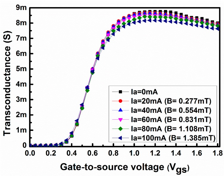
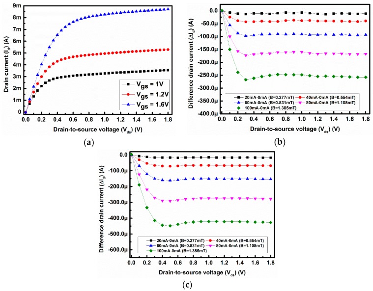
A novel concept of drain current modelling in rectangular normal MOS transistors with the Lorentz force has been proposed for the first time. The single-drain MOS transistor is qualified as a magnetic sensor. To create the Lorentz force, a DC loop current is applied through an on-chip metal loop around the device, and the relation between the applied loop current and the created magnetic field is assumed to be linear in nature. The drain current of the MOS transistor is reduced with the applied Lorentz force from both directions. This change in the drain current is ascribed to a change in mobility in the strong inversion region, and a change in mobility of around 4.45% is observed. To model this change, a set of novel drain current equations, under the Lorentz force, for the strong inversion region has been proposed. A satisfactory agreement of an average error of less than 2% between the measured and the calculated drain currents under the magnetic field created by an on-chip metal loop is achieved.
首次提出了一种在具有洛伦兹力的矩形常规MOS晶体管中进行漏极电流建模的新方法。单漏极MOS晶体管被用作磁传感器。为了产生洛伦兹力,通过器件周围的片上金属环施加直流环路电流,并且假设施加的环路电流与产生的磁场之间的关系本质上是线性的。MOS晶体管的漏极电流在两个方向上都随着施加的洛伦兹力而减小。漏极电流的这种变化归因于强反型区迁移率的变化,并且观察到迁移率变化约4.45%。为了对这种变化进行建模,提出了一组在洛伦兹力作用下针对强反型区的新型漏极电流方程。在由片上金属环产生的磁场下,测量的漏极电流与计算的漏极电流之间实现了平均误差小于2%的良好一致性。