Sinnarasa Inthuga, Thimont Yohann, Presmanes Lionel, Barnabé Antoine, Tailhades Philippe
CIRIMAT, Université de Toulouse, CNRS, INPT, UPS, 118 route de Narbonne, F-31062 Toulouse CEDEX 9, France.
Nanomaterials (Basel). 2017 Jun 27;7(7):157. doi: 10.3390/nano7070157.
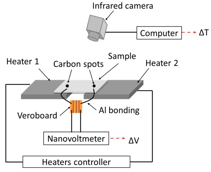
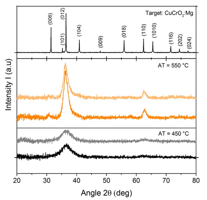
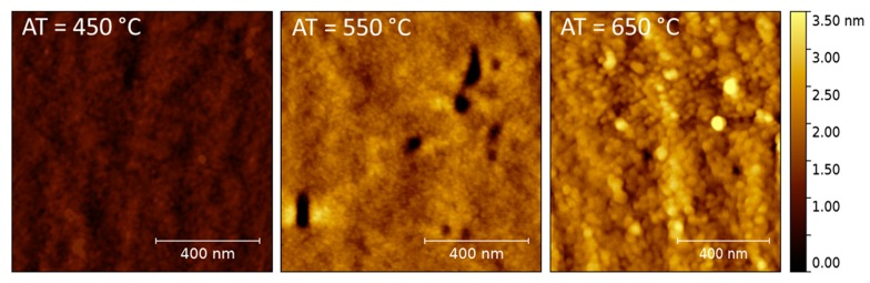
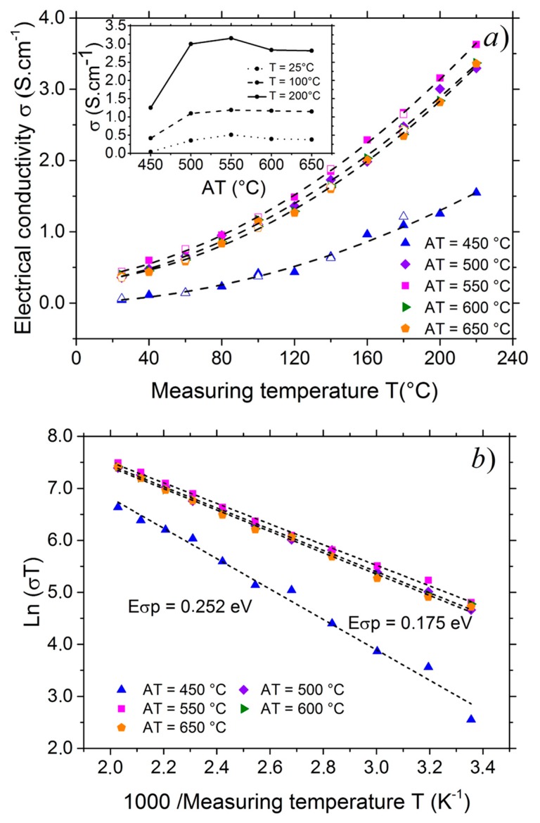
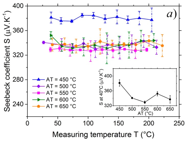
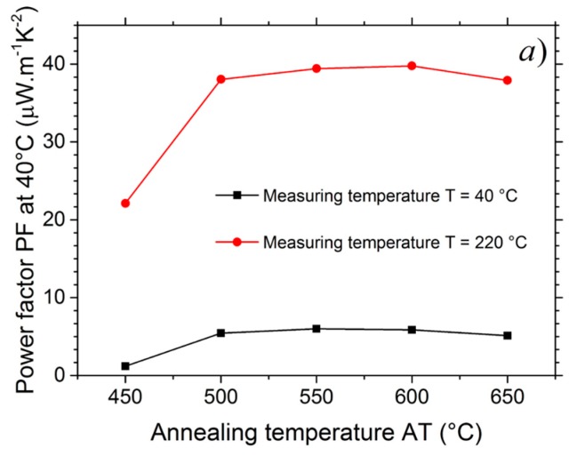
P-type Mg doped CuCrO₂ thin films have been deposited on fused silica substrates by Radio-Frequency (RF) magnetron sputtering. The as-deposited CuCrO₂:Mg thin films have been annealed at different temperatures (from 450 to 650 °C) under primary vacuum to obtain the delafossite phase. The annealed samples exhibit 3R delafossite structure. Electrical conductivity σ and Seebeck coefficient S of all annealed films have been measured from 40 to 220 °C. The optimized properties have been obtained for CuCrO₂:Mg thin film annealed at 550 °C. At a measurement temperature of 40 °C, this sample exhibited the highest electrical conductivity of 0.60 S·cm with a Seebeck coefficient of +329 µV·K. The calculated power factor ( = ²) was 6 µW·m·K at 40 °C and due to the constant Seebeck coefficient and the increasing electrical conductivity with measurement temperature, it reached 38 µW·m·K at 220 °C. Moreover, according to measurement of the Seebeck coefficient and electrical conductivity in temperature, we confirmed that CuCrO₂:Mg exhibits hopping conduction and degenerates semiconductor behavior. Carrier concentration, Fermi level, and hole effective mass have been discussed.
通过射频(RF)磁控溅射在熔融石英衬底上沉积了P型Mg掺杂的CuCrO₂薄膜。将沉积后的CuCrO₂:Mg薄膜在初级真空下于不同温度(450至650°C)进行退火,以获得铜铁矿相。退火后的样品呈现出3R铜铁矿结构。在40至220°C范围内测量了所有退火薄膜的电导率σ和塞贝克系数S。对于在550°C退火的CuCrO₂:Mg薄膜,获得了优化的性能。在40°C的测量温度下,该样品表现出最高电导率0.60 S·cm,塞贝克系数为+329 μV·K。计算得到的功率因子(=σ²)在40°C时为6 μW·m·K,并且由于塞贝克系数恒定以及电导率随测量温度升高,在220°C时达到38 μW·m·K。此外,根据温度下塞贝克系数和电导率的测量,我们证实CuCrO₂:Mg表现出跳跃传导和简并半导体行为。讨论了载流子浓度、费米能级和空穴有效质量。