Hamza Sarah, Ignaszak Anna, Kiani Amirkianoosh
Department of Mechanical Engineering, Silicon Hall: Laser Micro/Nano Fabrication Facility, University of New Brunswick, New Brunswick, E3B 5A3, Canada.
Department of Chemistry, University of New Brunswick, New Brunswick, E3B 5A3, Canada.
Nanoscale Res Lett. 2017 Dec;12(1):432. doi: 10.1186/s11671-017-2200-z. Epub 2017 Jun 30.
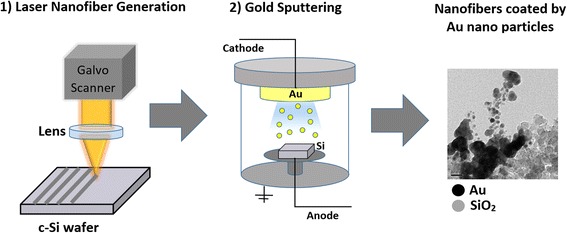
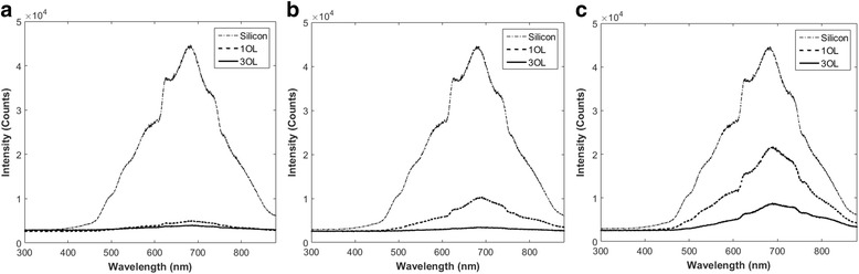
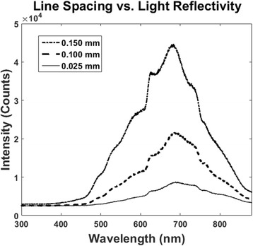
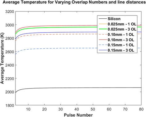
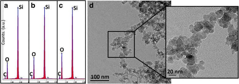
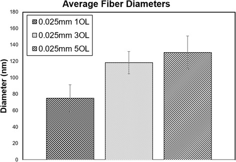
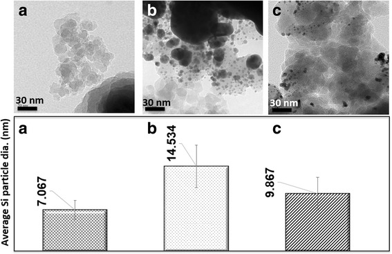
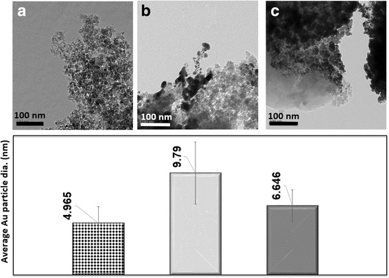
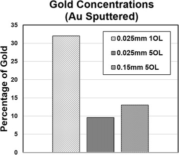
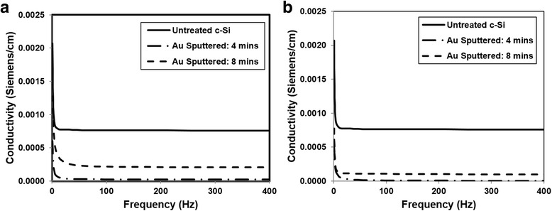
Biocompatible-sensing materials hold an important role in biomedical applications where there is a need to translate biological responses into electrical signals. Increasing the biocompatibility of these sensing devices generally causes a reduction in the overall conductivity due to the processing techniques. Silicon is becoming a more feasible and available option for use in these applications due to its semiconductor properties and availability. When processed to be porous, it has shown promising biocompatibility; however, a reduction in its conductivity is caused by its oxidization. To overcome this, gold embedding through sputtering techniques are proposed in this research as a means of controlling and further imparting electrical properties to laser induced silicon oxide nanofibers. Single crystalline silicon wafers were laser processed using an Nd:YAG pulsed nanosecond laser system at different laser parameters before undergoing gold sputtering. Controlling the scanning parameters (e.g., smaller line spacings) was found to induce the formation of nanofibrous structures, whose diameters grew with increasing overlaps (number of laser beam scanning through the same path). At larger line spacings, nano and microparticle formation was observed. Overlap (OL) increases led to higher light absorbance's by the wafers. The gold sputtered samples resulted in greater conductivities at higher gold concentrations, especially in samples with smaller fiber sizes. Overall, these findings show promising results for the future of silicon as a semiconductor and a biocompatible material for its use and development in the improvement of sensing applications.
生物相容性传感材料在生物医学应用中发挥着重要作用,在这些应用中需要将生物反应转化为电信号。由于加工技术的原因,提高这些传感设备的生物相容性通常会导致整体导电性降低。硅因其半导体特性和可用性,正成为这些应用中更可行且可用的选择。当加工成多孔结构时,它已显示出良好的生物相容性;然而,其氧化会导致导电性降低。为克服这一问题,本研究提出通过溅射技术嵌入金,作为控制并进一步赋予激光诱导氧化硅纳米纤维电学性能的一种方法。在进行金溅射之前,使用Nd:YAG脉冲纳秒激光系统在不同激光参数下对单晶硅片进行激光加工。发现控制扫描参数(例如,更小的线间距)会诱导纳米纤维结构的形成,其直径随着重叠度(激光束通过同一路径扫描的次数)的增加而增大。在较大的线间距下,观察到纳米和微粒的形成。重叠度(OL)的增加导致晶片的吸光度更高。在较高金浓度下,尤其是在纤维尺寸较小的样品中,溅射金的样品具有更高的导电性。总体而言,这些发现为硅作为一种半导体以及生物相容性材料在改善传感应用中的使用和开发前景显示出了令人期待的结果。