• 文献检索
  • 文档翻译
  • 深度研究
  • 学术资讯
  • Suppr Zotero 插件Zotero 插件
  • 邀请有礼
  • 套餐&价格
  • 历史记录
应用&插件
Suppr Zotero 插件Zotero 插件浏览器插件Mac 客户端Windows 客户端微信小程序
定价
高级版会员购买积分包购买API积分包
服务
文献检索文档翻译深度研究API 文档MCP 服务
关于我们
关于 Suppr公司介绍联系我们用户协议隐私条款
关注我们

Suppr 超能文献

核心技术专利:CN118964589B侵权必究
粤ICP备2023148730 号-1Suppr @ 2026

文献检索

告别复杂PubMed语法,用中文像聊天一样搜索,搜遍4000万医学文献。AI智能推荐,让科研检索更轻松。

立即免费搜索

文件翻译

保留排版,准确专业,支持PDF/Word/PPT等文件格式,支持 12+语言互译。

免费翻译文档

深度研究

AI帮你快速写综述,25分钟生成高质量综述,智能提取关键信息,辅助科研写作。

立即免费体验

一种采用标准背照式工艺制造的3.0μm三增益像素的90dB以上场景内单曝光动态范围CMOS图像传感器。

An Over 90 dB Intra-Scene Single-Exposure Dynamic Range CMOS Image Sensor Using a 3.0 μm Triple-Gain Pixel Fabricated in a Standard BSI Process.

作者信息

Takayanagi Isao, Yoshimura Norio, Mori Kazuya, Matsuo Shinichiro, Tanaka Shunsuke, Abe Hirofumi, Yasuda Naoto, Ishikawa Kenichiro, Okura Shunsuke, Ohsawa Shinji, Otaka Toshinori

机构信息

Brillnics Japan Inc., 6-21-12 Minami-Oi, Shinagawa-ku, Tokyo 140-0013, Japan.

出版信息

Sensors (Basel). 2018 Jan 12;18(1):203. doi: 10.3390/s18010203.

DOI:10.3390/s18010203
PMID:29329210
原文链接:https://pmc.ncbi.nlm.nih.gov/articles/PMC5796480/
Abstract

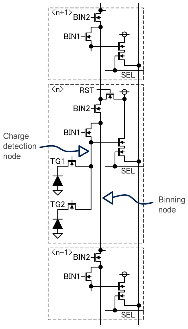
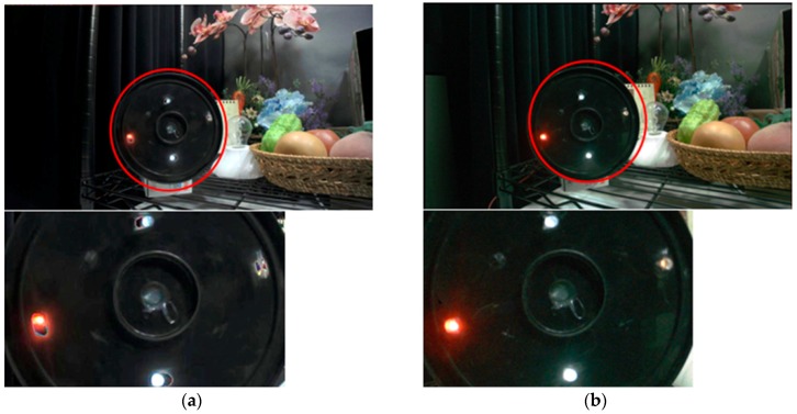
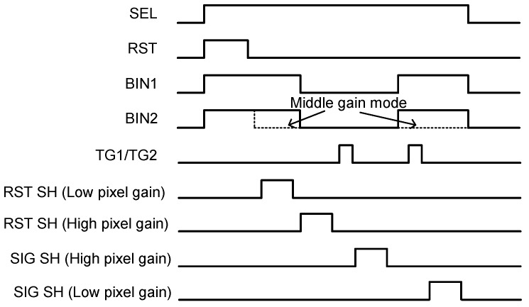
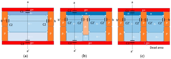
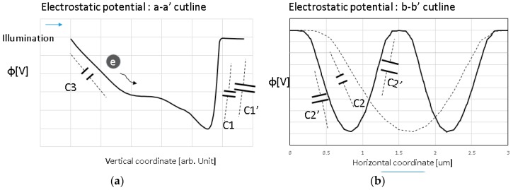
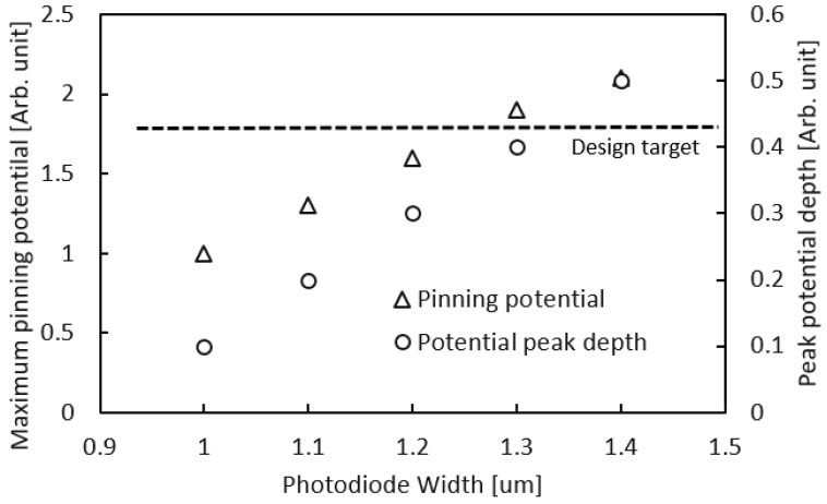
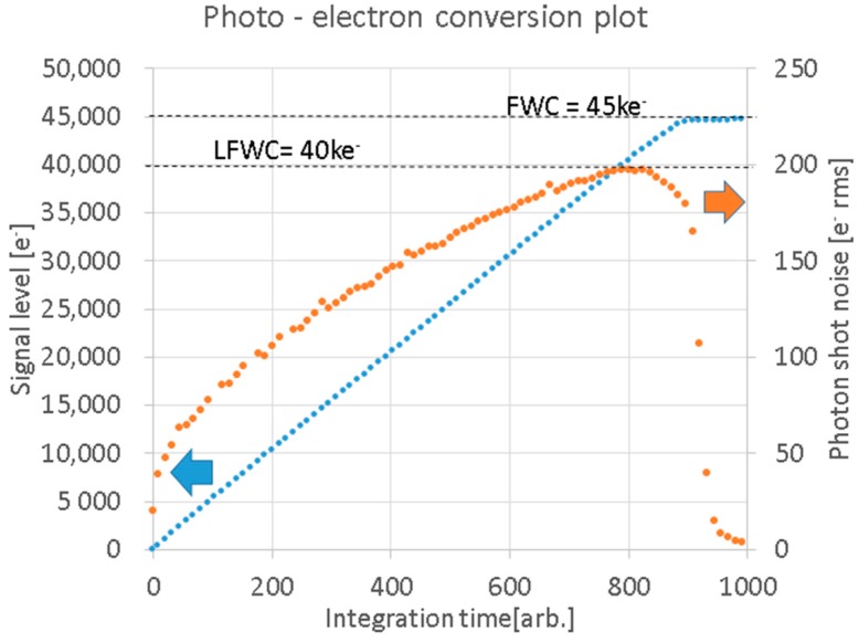
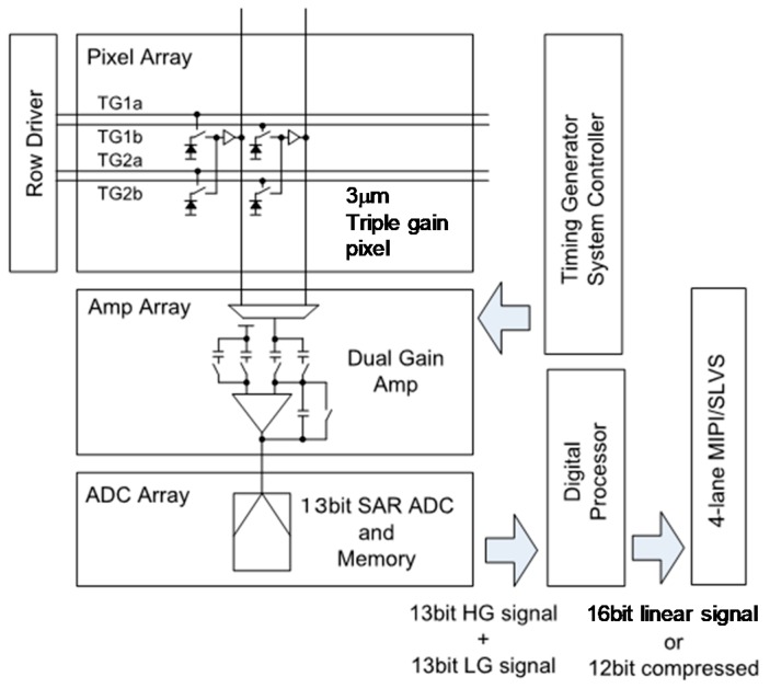
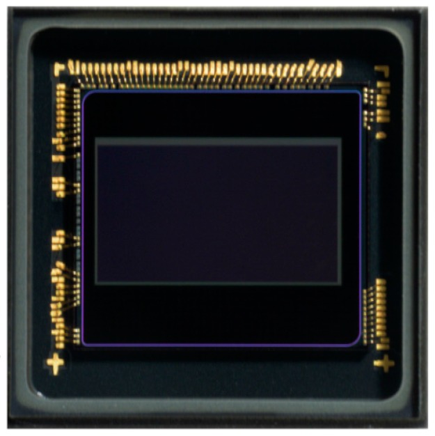
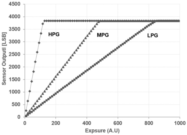
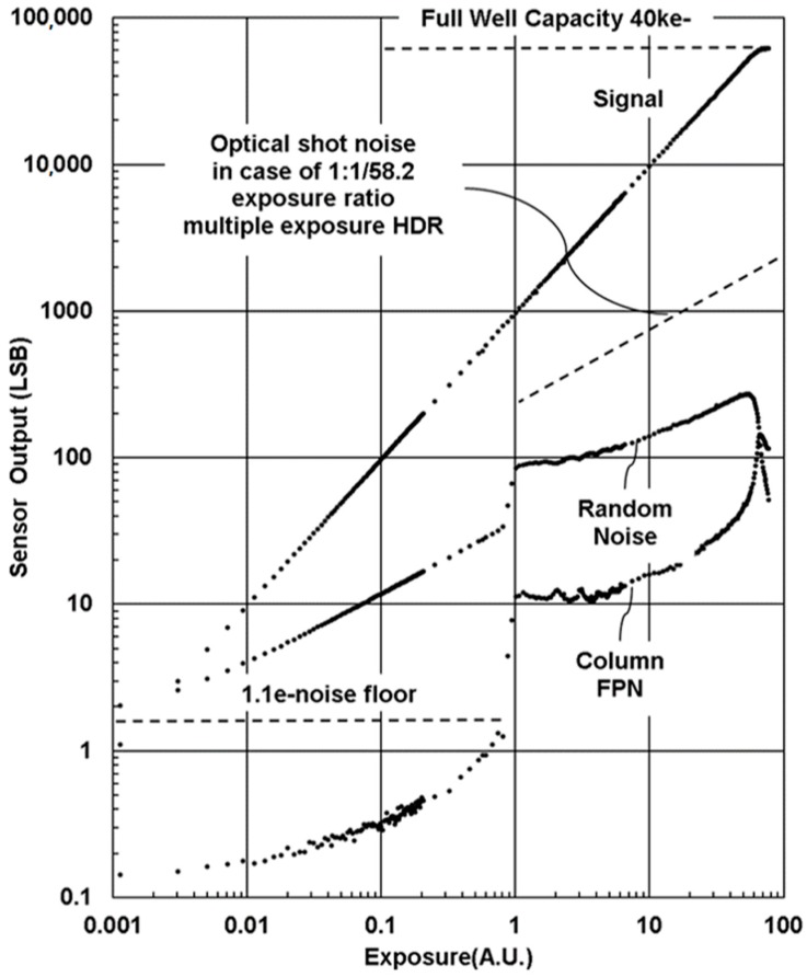
To respond to the high demand for high dynamic range imaging suitable for moving objects with few artifacts, we have developed a single-exposure dynamic range image sensor by introducing a triple-gain pixel and a low noise dual-gain readout circuit. The developed 3 μm pixel is capable of having three conversion gains. Introducing a new split-pinned photodiode structure, linear full well reaches 40 ke. Readout noise under the highest pixel gain condition is 1 e with a low noise readout circuit. Merging two signals, one with high pixel gain and high analog gain, and the other with low pixel gain and low analog gain, a single exposure dynamic rage (SEHDR) signal is obtained. Using this technology, a 1/2.7", 2M-pixel CMOS image sensor has been developed and characterized. The image sensor also employs an on-chip linearization function, yielding a 16-bit linear signal at 60 fps, and an intra-scene dynamic range of higher than 90 dB was successfully demonstrated. This SEHDR approach inherently mitigates the artifacts from moving objects or time-varying light sources that can appear in the multiple exposure high dynamic range (MEHDR) approach.

摘要

为了满足对适用于移动物体且伪像少的高动态范围成像的高需求,我们通过引入三增益像素和低噪声双增益读出电路,开发了一种单曝光动态范围图像传感器。所开发的3μm像素能够具有三种转换增益。引入新的分裂 pinned 光电二极管结构,线性满阱达到40ke。在最高像素增益条件下,使用低噪声读出电路时读出噪声为1e。将一个具有高像素增益和高模拟增益的信号与另一个具有低像素增益和低模拟增益的信号合并,可获得单曝光动态范围(SEHDR)信号。利用该技术,已开发并表征了一款1/2.7英寸、200万像素的CMOS图像传感器。该图像传感器还采用了片上线性化功能,可在60fps时产生16位线性信号,并成功展示了高于90dB的场景内动态范围。这种SEHDR方法从本质上减轻了多曝光高动态范围(MEHDR)方法中可能出现的移动物体或时变光源产生的伪像。

https://cdn.ncbi.nlm.nih.gov/pmc/blobs/88e0/5796480/174504343944/sensors-18-00203-g011.jpg
https://cdn.ncbi.nlm.nih.gov/pmc/blobs/88e0/5796480/f5772b1bf5e8/sensors-18-00203-g001.jpg
https://cdn.ncbi.nlm.nih.gov/pmc/blobs/88e0/5796480/2b98821d8016/sensors-18-00203-g002.jpg
https://cdn.ncbi.nlm.nih.gov/pmc/blobs/88e0/5796480/85aa11ad9d36/sensors-18-00203-g003.jpg
https://cdn.ncbi.nlm.nih.gov/pmc/blobs/88e0/5796480/b22002c80114/sensors-18-00203-g004.jpg
https://cdn.ncbi.nlm.nih.gov/pmc/blobs/88e0/5796480/3a4b08153994/sensors-18-00203-g005.jpg
https://cdn.ncbi.nlm.nih.gov/pmc/blobs/88e0/5796480/f5a23e62b5c7/sensors-18-00203-g006.jpg
https://cdn.ncbi.nlm.nih.gov/pmc/blobs/88e0/5796480/6f4f3de584c5/sensors-18-00203-g007.jpg
https://cdn.ncbi.nlm.nih.gov/pmc/blobs/88e0/5796480/9d4c7e67d354/sensors-18-00203-g008.jpg
https://cdn.ncbi.nlm.nih.gov/pmc/blobs/88e0/5796480/a1d03bb0ae05/sensors-18-00203-g009.jpg
https://cdn.ncbi.nlm.nih.gov/pmc/blobs/88e0/5796480/0c22bd1ff0bd/sensors-18-00203-g010.jpg
https://cdn.ncbi.nlm.nih.gov/pmc/blobs/88e0/5796480/174504343944/sensors-18-00203-g011.jpg

相似文献

1
An Over 90 dB Intra-Scene Single-Exposure Dynamic Range CMOS Image Sensor Using a 3.0 μm Triple-Gain Pixel Fabricated in a Standard BSI Process.一种采用标准背照式工艺制造的3.0μm三增益像素的90dB以上场景内单曝光动态范围CMOS图像传感器。
Sensors (Basel). 2018 Jan 12;18(1):203. doi: 10.3390/s18010203.
2
A Stacked Back Side-Illuminated Voltage Domain Global Shutter CMOS Image Sensor with a 4.0 μm Multiple Gain Readout Pixel .一种堆叠背照式电压域全局快门 CMOS 图像传感器,具有 4.0μm 多增益读出像素。
Sensors (Basel). 2020 Jan 15;20(2):486. doi: 10.3390/s20020486.
3
Automotive 2.1 μm Full-Depth Deep Trench Isolation CMOS Image Sensor with a 120 dB Single-Exposure Dynamic Range.具有120dB单曝光动态范围的汽车级2.1μm全深度深沟槽隔离CMOS图像传感器。
Sensors (Basel). 2023 Nov 13;23(22):9150. doi: 10.3390/s23229150.
4
A 120-ke Full-Well Capacity 160-µV/e Conversion Gain 2.8-µm Backside-Illuminated Pixel with a Lateral Overflow Integration Capacitor.一款 120ke 全阱容量、160µV/e 转换增益、2.8µm 背照式像素、具有横向溢流积分电容的器件。
Sensors (Basel). 2019 Dec 17;19(24):5572. doi: 10.3390/s19245572.
5
QLog Solar-Cell Mode Photodiode Logarithmic CMOS Pixel Using Charge Compression and Readout.采用电荷压缩和读出技术的QLog太阳能电池模式光电二极管对数CMOS像素
Sensors (Basel). 2018 Feb 14;18(2):584. doi: 10.3390/s18020584.
6
A Dynamic Range Enhanced Readout Technique with a Two-Step TDC for High Speed Linear CMOS Image Sensors.一种用于高速线性CMOS图像传感器的具有两步TDC的动态范围增强读出技术。
Sensors (Basel). 2015 Nov 6;15(11):28224-43. doi: 10.3390/s151128224.
7
A 75-ps Gated CMOS Image Sensor with Low Parasitic Light Sensitivity.一款具有低寄生光灵敏度的75皮秒门控CMOS图像传感器。
Sensors (Basel). 2016 Jun 29;16(7):999. doi: 10.3390/s16070999.
8
Statistical Analysis of the Random Telegraph Noise in a 1.1 μm Pixel, 8.3 MP CMOS Image Sensor Using On-Chip Time Constant Extraction Method.采用片上时间常数提取方法对1.1μm像素、830万像素CMOS图像传感器中的随机电报噪声进行统计分析
Sensors (Basel). 2017 Nov 23;17(12):2704. doi: 10.3390/s17122704.
9
A 316MP, 120FPS, High Dynamic Range CMOS Image Sensor for Next Generation Immersive Displays.一款用于下一代沉浸式显示器的316MP、120FPS、高动态范围CMOS图像传感器。
Sensors (Basel). 2023 Oct 11;23(20):8383. doi: 10.3390/s23208383.
10
Development of Gated Pinned Avalanche Photodiode Pixels for High-Speed Low-Light Imaging.用于高速低光成像的门控 pinned 雪崩光电二极管像素的开发。
Sensors (Basel). 2016 Aug 15;16(8):1294. doi: 10.3390/s16081294.

引用本文的文献

1
A Thin-Film Pinned-Photodiode Imager Pixel with Fully Monolithic Fabrication and beyond 1Me- Full Well Capacity.一种具有全单片制造工艺且满阱容量超过1Me的薄膜 pinned 光电二极管成像器像素。
Sensors (Basel). 2023 Oct 29;23(21):8803. doi: 10.3390/s23218803.
2
A 316MP, 120FPS, High Dynamic Range CMOS Image Sensor for Next Generation Immersive Displays.一款用于下一代沉浸式显示器的316MP、120FPS、高动态范围CMOS图像传感器。
Sensors (Basel). 2023 Oct 11;23(20):8383. doi: 10.3390/s23208383.
3
An Area-Efficient up/down Double-Sampling Circuit for a LOFIC CMOS Image Sensor.
一种用于 LOFIC CMOS 图像传感器的高效能上下双取样电路。
Sensors (Basel). 2023 May 4;23(9):4478. doi: 10.3390/s23094478.
4
A Stacked Back Side-Illuminated Voltage Domain Global Shutter CMOS Image Sensor with a 4.0 μm Multiple Gain Readout Pixel .一种堆叠背照式电压域全局快门 CMOS 图像传感器,具有 4.0μm 多增益读出像素。
Sensors (Basel). 2020 Jan 15;20(2):486. doi: 10.3390/s20020486.
5
A 120-ke Full-Well Capacity 160-µV/e Conversion Gain 2.8-µm Backside-Illuminated Pixel with a Lateral Overflow Integration Capacitor.一款 120ke 全阱容量、160µV/e 转换增益、2.8µm 背照式像素、具有横向溢流积分电容的器件。
Sensors (Basel). 2019 Dec 17;19(24):5572. doi: 10.3390/s19245572.