Department of Electronic Engineering, College of Electrical and Computer Engineering, Chungbuk National University, Cheongju 28644, Korea.
Department of Electronics, National Telecommunication Institute, Nasr City, Cairo 11768, Egypt.
Sensors (Basel). 2018 Jul 8;18(7):2200. doi: 10.3390/s18072200.
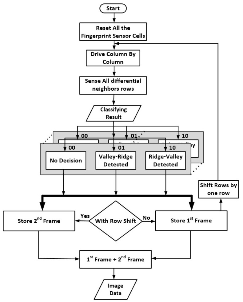
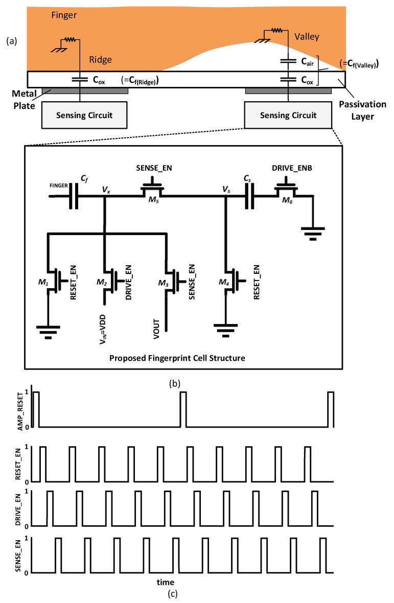
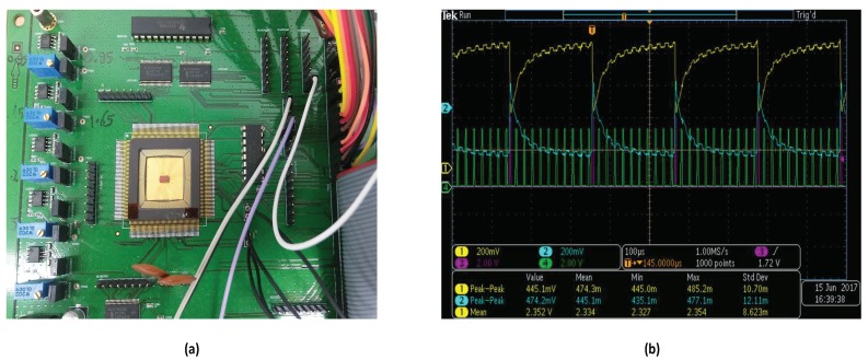
In this paper, we introduce a differential sensing technique for CMOS capacitive fingerprint detection. It employs a new capacitive-sensing cell structure with charge sharing detection and readout circuit. The proposed technique also can eliminate the effect of parasitic capacitances by employing parasitic insensitive switched-capacitor structure and so increases the sensitivity even under severe noisy conditions. It can also overcome the performance degradation caused by various conditions of finger surface by using a differential integrator and adjusting its number of integrations. In addition, the proposed architecture allows parallel detection of all sensing channels. It can, therefore, substantially speed up the detection process compared with conventional architectures. We implemented a prototype fingerprint sensor chip with an array of 20 × 16 sensor cells using a 130 nm CMOS process. Simulation experiments demonstrated that the proposed architecture provided an SNR gain of 54 dB, whereas a conventional single line sensing gives an SNR gain of only 13 dB.
在本文中,我们介绍了一种用于 CMOS 电容式指纹检测的差分感应技术。它采用了一种具有电荷共享检测和读出电路的新型电容感应单元结构。所提出的技术还可以通过采用寄生不敏感开关电容结构来消除寄生电容的影响,从而即使在严重噪声条件下也能提高灵敏度。它还可以通过使用差分积分器和调整其积分次数来克服由各种手指表面条件引起的性能下降。此外,所提出的架构允许所有感应通道的并行检测。因此,与传统架构相比,它可以大大加快检测过程。我们使用 130nm CMOS 工艺实现了一个具有 20×16 个传感器单元的阵列的指纹传感器芯片原型。仿真实验表明,所提出的架构提供了 54dB 的 SNR 增益,而传统的单线感应仅提供 13dB 的 SNR 增益。