Zheng Ze-Bo, Li Jun-Tao, Ma Teng, Fang Han-Lin, Ren Wen-Cai, Chen Jun, She Jun-Cong, Zhang Yu, Liu Fei, Chen Huan-Jun, Deng Shao-Zhi, Xu Ning-Sheng
State Key Laboratory of Optoelectronic Materials and Technologies, Guangdong Province Key Laboratory of Display Material and Technology, School of Electronics and Information Technology, Guangzhou 510275, China.
State Key Laboratory of Optoelectronic Materials and Technologies, School of Physics, Sun Yat-sen University, Guangzhou 510275, China.
Light Sci Appl. 2017 Oct 6;6(10):e17057. doi: 10.1038/lsa.2017.57. eCollection 2017 Oct.
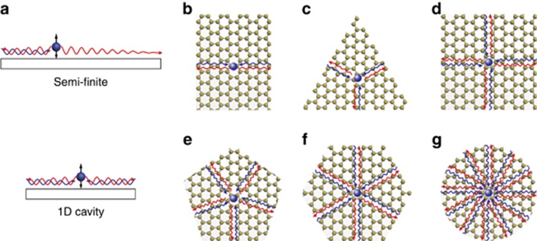
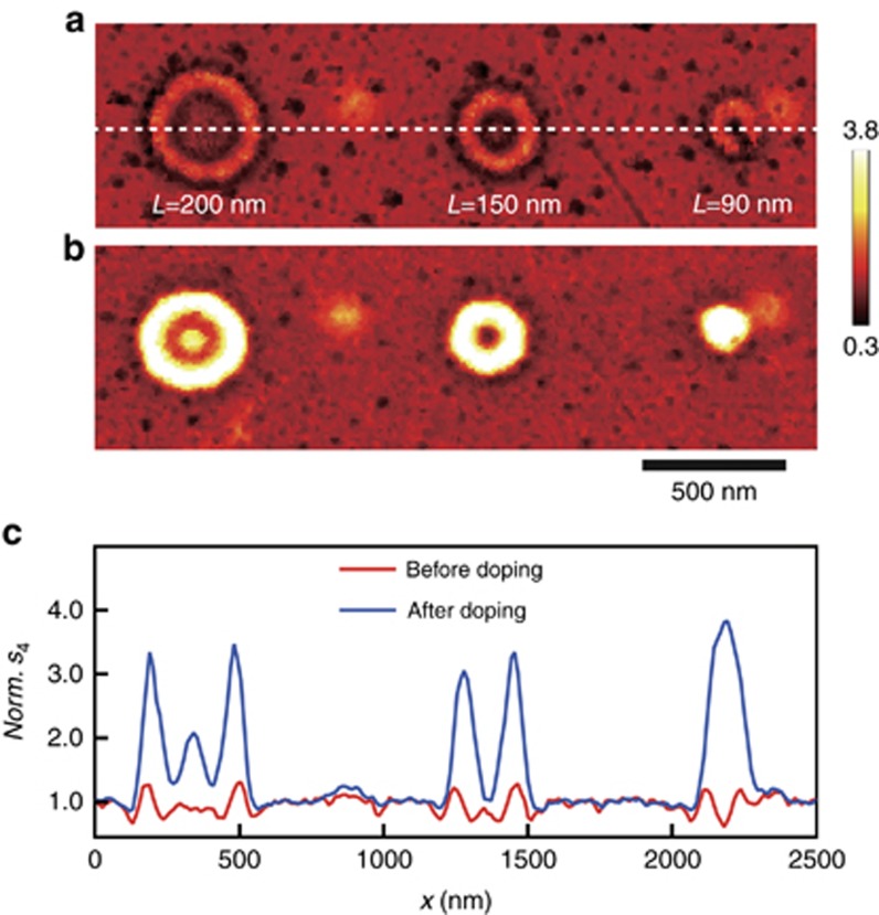
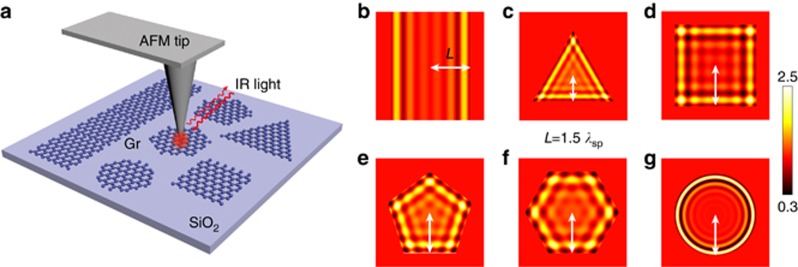
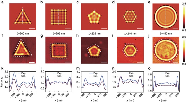
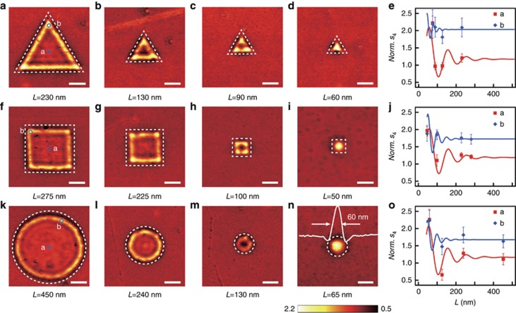
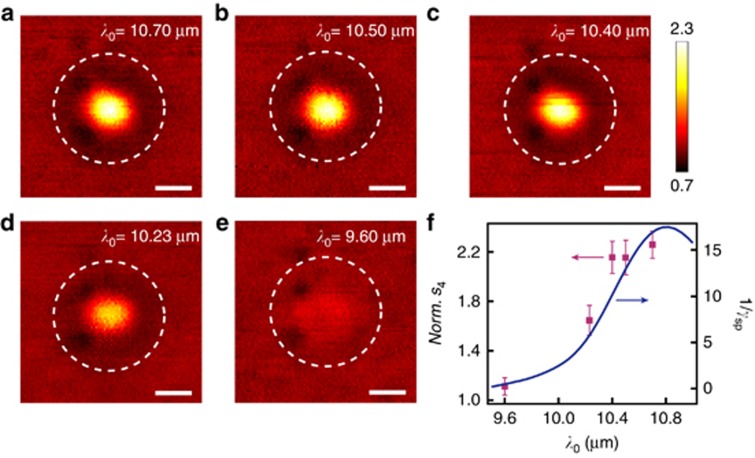
Graphene has great potential for enhancing light-matter interactions in a two-dimensional regime due to surface plasmons with low loss and strong light confinement. Further utilization of graphene in nanophotonics relies on the precise control of light localization properties. Here, we demonstrate the tailoring of electromagnetic field localizations in the mid-infrared region by precisely shaping the graphene into nanostructures with different geometries. We generalize the phenomenological cavity model and employ nanoimaging techniques to quantitatively calculate and experimentally visualize the two-dimensional electromagnetic field distributions within the nanostructures, which indicate that the electromagnetic field can be shaped into specific patterns depending on the shapes and sizes of the nanostructures. Furthermore, we show that the light localization performance can be further improved by reducing the sizes of the nanostructures, where a lateral confinement of /180 of the incidence light can be achieved. The electromagnetic field localizations within a nanostructure with a specific geometry can also be modulated by chemical doping. Our strategies can, in principle, be generalized to other two-dimensional materials, therefore providing new degrees of freedom for designing nanophotonic components capable of tailoring two-dimensional light confinement over a broad wavelength range.
由于具有低损耗和强光限制的表面等离子体,石墨烯在二维体系中增强光与物质相互作用方面具有巨大潜力。石墨烯在纳米光子学中的进一步应用依赖于对光局域特性的精确控制。在此,我们通过将石墨烯精确地塑造为具有不同几何形状的纳米结构,展示了在中红外区域对电磁场局域的调控。我们推广了唯象腔模型,并采用纳米成像技术定量计算和实验可视化纳米结构内的二维电磁场分布,这表明电磁场可根据纳米结构的形状和尺寸被塑造为特定模式。此外,我们表明通过减小纳米结构的尺寸可进一步提高光局域性能,在此可实现入射光/180的横向限制。具有特定几何形状的纳米结构内的电磁场局域也可通过化学掺杂进行调制。我们的策略原则上可推广到其他二维材料,从而为设计能够在宽波长范围内调控二维光限制的纳米光子学组件提供了新的自由度。