Park Jun-Young, Kim Weon-Guk, Bae Hagyoul, Jin Ik Kyeong, Kim Da-Jin, Im Hwon, Tcho Il-Woong, Choi Yang-Kyu
School of Electrical Engineering, Korea Advanced Institute of Science and Technology, (KAIST) 291 Daehak-ro, Yuseong-gu, Daejeon, 34141, Republic of Korea.
Sci Rep. 2018 Oct 8;8(1):14953. doi: 10.1038/s41598-018-33309-x.
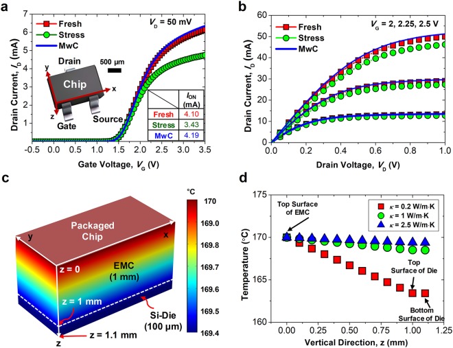
Microwave-induced thermal curing is demonstrated to improve the reliability and to prolong the lifetime of chips containing nanoscale electron devices. A film containing graphite powder with high microwave absorbing efficiency was fabricated at low cost. The film is flexible, bendable, foldable, and attachable to a chip. A commercial off-the-shelf chip and a representative 3-dimensional (3D) metal-oxide-semiconductor field-effect transistor (MOSFET), known as FinFET, were utilized to verify the curing behaviors of the microwave-induced heat treatment. The heat effectively cured not only total ionizing dose (TID) damage from the external environment, but also internal electrical stress such as hot-carrier injection (HCI), which are representative sources of damages in MOSFET insulators. Then, the characteristics of the pre- and post-curing electron devices are investigated using electrical measurements and numerical simulations.
微波诱导热固化被证明可以提高包含纳米级电子器件的芯片的可靠性并延长其寿命。以低成本制备了一种具有高微波吸收效率的含石墨粉薄膜。该薄膜具有柔韧性、可弯曲、可折叠且可附着在芯片上。使用商用现货芯片和一种典型的三维(3D)金属氧化物半导体场效应晶体管(MOSFET),即鳍式场效应晶体管(FinFET),来验证微波诱导热处理的固化行为。热量不仅有效固化了来自外部环境的总电离剂量(TID)损伤,还固化了诸如热载流子注入(HCI)等内部电应力,这些是MOSFET绝缘体中典型的损伤源。然后,通过电学测量和数值模拟研究了固化前后电子器件的特性。