Jia Chuancheng, Famili Marjan, Carlotti Marco, Liu Yuan, Wang Peiqi, Grace Iain M, Feng Ziying, Wang Yiliu, Zhao Zipeng, Ding Mengning, Xu Xiang, Wang Chen, Lee Sung-Joon, Huang Yu, Chiechi Ryan C, Lambert Colin J, Duan Xiangfeng
Department of Chemistry and Biochemistry, University of California, Los Angeles, Los Angeles, CA 90095, USA.
Physics Department, Lancaster University, Lancaster LA1 4YB, UK.
Sci Adv. 2018 Oct 12;4(10):eaat8237. doi: 10.1126/sciadv.aat8237. eCollection 2018 Oct.
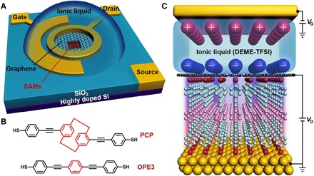
Molecular transistors operating in the quantum tunneling regime represent potential electronic building blocks for future integrated circuits. However, due to their complex fabrication processes and poor stability, traditional molecular transistors can only operate stably at cryogenic temperatures. Here, through a combined experimental and theoretical investigation, we demonstrate a new design of vertical molecular tunneling transistors, with stable switching operations up to room temperature, formed from cross-plane graphene/self-assembled monolayer (SAM)/gold heterostructures. We show that vertical molecular junctions formed from pseudo--bis((4-(acetylthio)phenyl)ethynyl)--[2,2]cyclophane (PCP) SAMs exhibit destructive quantum interference (QI) effects, which are absent in 1,4-bis(((4-acetylthio)phenyl)ethynyl)benzene (OPE3) SAMs. Consequently, the zero-bias differential conductance of the former is only about 2% of the latter, resulting in an enhanced on-off current ratio for (PCP) SAMs. Field-effect control is achieved using an ionic liquid gate, whose strong vertical electric field penetrates through the graphene layer and tunes the energy levels of the SAMs. The resulting on-off current ratio achieved in PCP SAMs can reach up to ~330, about one order of magnitude higher than that of OPE3 SAMs. The demonstration of molecular junctions with combined QI effect and gate tunability represents a critical step toward functional devices in future molecular-scale electronics.
工作在量子隧穿 regime 的分子晶体管是未来集成电路潜在的电子构建模块。然而,由于其复杂的制造工艺和较差的稳定性,传统分子晶体管只能在低温下稳定工作。在此,通过实验和理论相结合的研究,我们展示了一种新型垂直分子隧穿晶体管的设计,它由跨平面石墨烯/自组装单分子层(SAM)/金异质结构组成,在室温下具有稳定的开关操作。我们表明,由伪 - 双((4 - (乙酰硫基)苯基)乙炔基) - [2,2]环芳(PCP)SAMs 形成的垂直分子结表现出破坏性量子干涉(QI)效应,而在 1,4 - 双(((4 - 乙酰硫基)苯基)乙炔基)苯(OPE3)SAMs 中不存在这种效应。因此,前者的零偏置微分电导仅约为后者的 2%,导致(PCP)SAMs 的开 - 关电流比增强。使用离子液体栅极实现场效应控制,其强垂直电场穿透石墨烯层并调节 SAMs 的能级。在 PCP SAMs 中实现的开 - 关电流比可高达约 330,比 OPE3 SAMs 高约一个数量级。具有组合 QI 效应和栅极可调性的分子结的证明是迈向未来分子尺度电子学中功能器件的关键一步。