• 文献检索
  • 文档翻译
  • 深度研究
  • 学术资讯
  • Suppr Zotero 插件Zotero 插件
  • 邀请有礼
  • 套餐&价格
  • 历史记录
应用&插件
Suppr Zotero 插件Zotero 插件浏览器插件Mac 客户端Windows 客户端微信小程序
定价
高级版会员购买积分包购买API积分包
服务
文献检索文档翻译深度研究API 文档MCP 服务
关于我们
关于 Suppr公司介绍联系我们用户协议隐私条款
关注我们

Suppr 超能文献

核心技术专利:CN118964589B侵权必究
粤ICP备2023148730 号-1Suppr @ 2026

文献检索

告别复杂PubMed语法,用中文像聊天一样搜索,搜遍4000万医学文献。AI智能推荐,让科研检索更轻松。

立即免费搜索

文件翻译

保留排版,准确专业,支持PDF/Word/PPT等文件格式,支持 12+语言互译。

免费翻译文档

深度研究

AI帮你快速写综述,25分钟生成高质量综述,智能提取关键信息,辅助科研写作。

立即免费体验

用于微波和毫米波应用的超薄熔融石英晶圆中通孔的制造

Fabrication of Through via Holes in Ultra-Thin Fused Silica Wafers for Microwave and Millimeter-Wave Applications.

作者信息

Li Xiao, Chan King Yuk, Ramer Rodica

机构信息

School of Electrical Engineering and Telecommunications, University of New South Wales, Sydney, NSW 2052, Australia.

出版信息

Micromachines (Basel). 2018 Mar 20;9(3):138. doi: 10.3390/mi9030138.

DOI:10.3390/mi9030138
PMID:30424072
原文链接:https://pmc.ncbi.nlm.nih.gov/articles/PMC6187369/
Abstract

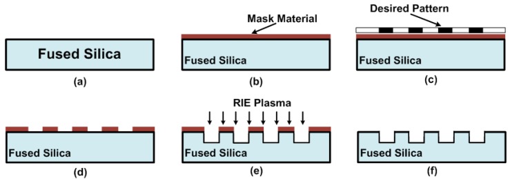
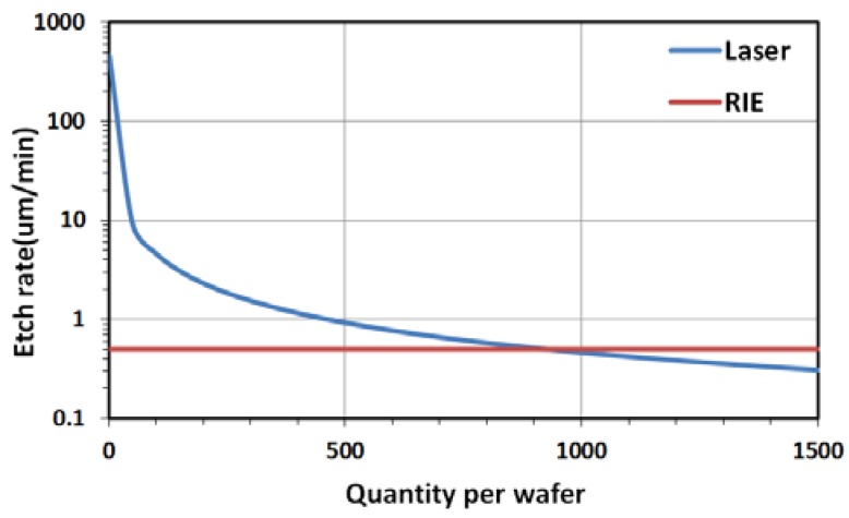
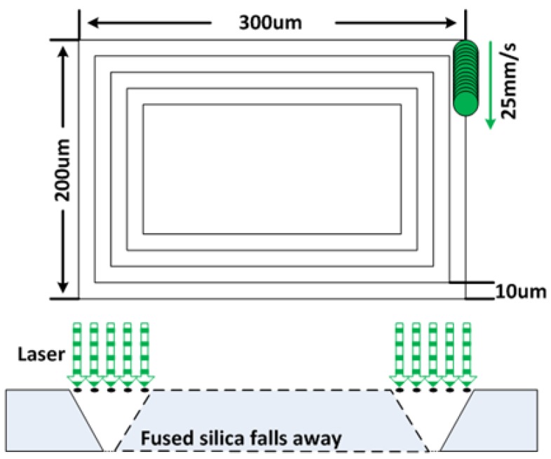
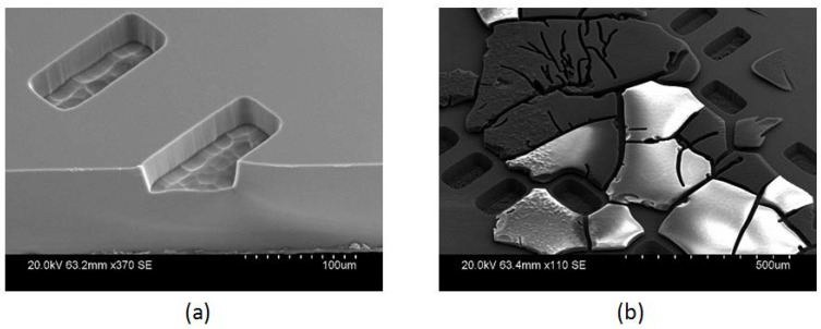
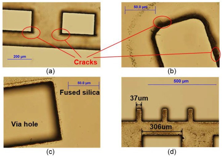
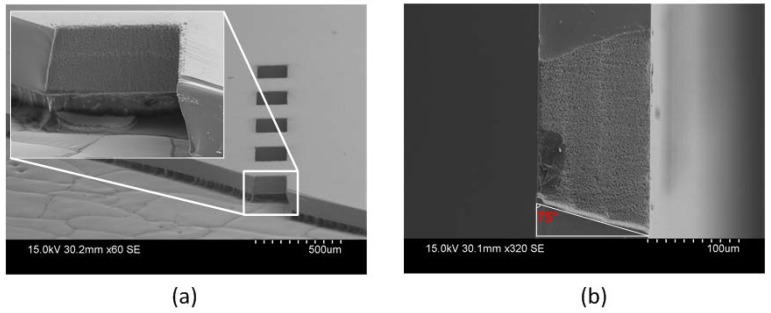
Through via holes in fused silica are a key infrastructure element of microwave and millimeter-wave circuits and 3D integration. In this work, etching through via holes in ultra-thin fused silica wafers using deep reactive-ion etching (DRIE) and laser ablation was developed and analyzed. The experimental setup and process parameters for both methods are presented and compared. For DRIE, three types of mask materials including KMPR 1035 (Nippon Kayaku, Tokyo, Japan) photoresist, amorphous silicon and chromium-with their corresponding optimized processing recipes-were tested, aiming at etching through a 100 μm fused silica wafer. From the experiments, we concluded that using chromium as the masking material is the best choice when using DRIE. However, we found that the laser ablation method with a laser pulse fluence of 2.89 J/cm² and a pulse overlap of 91% has advantages over DRIE. The laser ablation method has a simpler process complexity, while offering a fair etching result. In particular, the sidewall profile angle is measured to be 75° to the bottom surface of the wafer, which is ideal for the subsequent metallization process. As a demonstration, a two-inch wafer with 624 via holes was processed using both technologies, and the laser ablation method showed better efficiency compared to DRIE.

摘要

贯穿熔融石英的通孔是微波和毫米波电路以及3D集成的关键基础设施元件。在这项工作中,开发并分析了使用深反应离子刻蚀(DRIE)和激光烧蚀在超薄熔融石英晶圆上刻蚀通孔的方法。介绍并比较了这两种方法的实验装置和工艺参数。对于DRIE,测试了三种掩膜材料,包括KMPR 1035(日本东京日东化成)光刻胶、非晶硅和铬以及它们相应的优化工艺配方,目标是刻蚀穿透100μm厚的熔融石英晶圆。通过实验,我们得出结论,在使用DRIE时,使用铬作为掩膜材料是最佳选择。然而,我们发现激光脉冲能量密度为2.89J/cm²且脉冲重叠率为91%的激光烧蚀方法比DRIE具有优势。激光烧蚀方法的工艺复杂度更低,同时蚀刻效果良好。特别是,测量到侧壁轮廓与晶圆底面的夹角为75°,这对于后续的金属化工艺来说是理想的。作为演示,使用这两种技术对一个带有624个通孔的两英寸晶圆进行了加工,结果表明激光烧蚀方法比DRIE具有更高的效率。

https://cdn.ncbi.nlm.nih.gov/pmc/blobs/1cf3/6187369/35a6f3a78dc4/micromachines-09-00138-g006.jpg
https://cdn.ncbi.nlm.nih.gov/pmc/blobs/1cf3/6187369/72a2b4613ace/micromachines-09-00138-g001.jpg
https://cdn.ncbi.nlm.nih.gov/pmc/blobs/1cf3/6187369/51b146f1c344/micromachines-09-00138-g002.jpg
https://cdn.ncbi.nlm.nih.gov/pmc/blobs/1cf3/6187369/10230c625039/micromachines-09-00138-g003.jpg
https://cdn.ncbi.nlm.nih.gov/pmc/blobs/1cf3/6187369/f24bc2ae5a11/micromachines-09-00138-g004.jpg
https://cdn.ncbi.nlm.nih.gov/pmc/blobs/1cf3/6187369/1e2f4178bf0f/micromachines-09-00138-g005.jpg
https://cdn.ncbi.nlm.nih.gov/pmc/blobs/1cf3/6187369/35a6f3a78dc4/micromachines-09-00138-g006.jpg

相似文献

1
Fabrication of Through via Holes in Ultra-Thin Fused Silica Wafers for Microwave and Millimeter-Wave Applications.用于微波和毫米波应用的超薄熔融石英晶圆中通孔的制造
Micromachines (Basel). 2018 Mar 20;9(3):138. doi: 10.3390/mi9030138.
2
Deep multilevel wet etching of fused silica glass microstructures in BOE solution.BOE 溶液中熔融石英玻璃微结构的深层多级湿法刻蚀。
Sci Rep. 2023 Mar 30;13(1):5228. doi: 10.1038/s41598-023-32503-w.
3
Deep reactive ion etched anti-reflection coatings for sub-millimeter silicon optics.用于亚毫米硅光学器件的深度反应离子蚀刻抗反射涂层。
Appl Opt. 2017 Apr 1;56(10):2796-2803. doi: 10.1364/AO.56.002796.
4
Fabrication of Substrate-Integrated Waveguide Using Micromachining of Photoetchable Glass Substrate for 5G Millimeter-Wave Applications.基于可光蚀刻玻璃基板微加工的5G毫米波应用衬底集成波导制造
Micromachines (Basel). 2023 Jan 22;14(2):288. doi: 10.3390/mi14020288.
5
Light transmission and internal scattering in pulsed laser-etched partially-transparent silicon wafers.脉冲激光蚀刻的部分透明硅片中的光传输与内部散射
Heliyon. 2019 Nov 20;5(11):e02790. doi: 10.1016/j.heliyon.2019.e02790. eCollection 2019 Nov.
6
Time multiplexed deep reactive ion etching of germanium and silicon-A comparison of mechanisms and application to x-ray optics.锗和硅的时间复用深度反应离子刻蚀——机理比较及在X射线光学中的应用
J Vac Sci Technol B Nanotechnol Microelectron. 2018 Jan;36(1):011205. doi: 10.1116/1.4991875. Epub 2018 Jan 4.
7
Reduced Etch Lag and High Aspect Ratios by Deep Reactive Ion Etching (DRIE).通过深反应离子刻蚀(DRIE)减少刻蚀延迟并实现高纵横比
Micromachines (Basel). 2021 May 10;12(5):542. doi: 10.3390/mi12050542.
8
Manufacturing of a Compact Micro Air Bearing Device for Power Micro Electro Mechanical System (MEMS) Applications Using Silica Film Assisted Processing.利用二氧化硅薄膜辅助工艺制造用于功率微机电系统(MEMS)应用的紧凑型微型空气轴承装置。
Micromachines (Basel). 2018 Apr 2;9(4):166. doi: 10.3390/mi9040166.
9
Wafer-scale fabrication of fused silica chips for low-noise recording of resistive pulses through nanopores.用于通过纳米孔进行电阻脉冲低噪声记录的熔融石英芯片的晶圆级制造。
Nanotechnology. 2019 Jun 28;30(26):265301. doi: 10.1088/1361-6528/ab0e2a. Epub 2019 Mar 8.
10
Millimeter-Wave Substrate Integrated Waveguide Using Micromachined Tungsten-Coated Through Glass Silicon Via Structures.采用微机械加工的镀钨玻璃通孔结构的毫米波基片集成波导
Micromachines (Basel). 2018 Apr 9;9(4):172. doi: 10.3390/mi9040172.

引用本文的文献

1
Recent Advances in Reactive Ion Etching and Applications of High-Aspect-Ratio Microfabrication.反应离子蚀刻的最新进展及高深宽比微纳加工的应用
Micromachines (Basel). 2021 Aug 20;12(8):991. doi: 10.3390/mi12080991.