• 文献检索
  • 文档翻译
  • 深度研究
  • 学术资讯
  • Suppr Zotero 插件Zotero 插件
  • 邀请有礼
  • 套餐&价格
  • 历史记录
应用&插件
Suppr Zotero 插件Zotero 插件浏览器插件Mac 客户端Windows 客户端微信小程序
定价
高级版会员购买积分包购买API积分包
服务
文献检索文档翻译深度研究API 文档MCP 服务
关于我们
关于 Suppr公司介绍联系我们用户协议隐私条款
关注我们

Suppr 超能文献

核心技术专利:CN118964589B侵权必究
粤ICP备2023148730 号-1Suppr @ 2026

文献检索

告别复杂PubMed语法,用中文像聊天一样搜索,搜遍4000万医学文献。AI智能推荐,让科研检索更轻松。

立即免费搜索

文件翻译

保留排版,准确专业,支持PDF/Word/PPT等文件格式,支持 12+语言互译。

免费翻译文档

深度研究

AI帮你快速写综述,25分钟生成高质量综述,智能提取关键信息,辅助科研写作。

立即免费体验

二氧化钒薄膜在六方氮化硼薄片上的生长作为可转移衬底。

Growth of vanadium dioxide thin films on hexagonal boron nitride flakes as transferrable substrates.

作者信息

Genchi Shingo, Yamamoto Mahito, Shigematsu Koji, Aritomi Shodai, Nouchi Ryo, Kanki Teruo, Watanabe Kenji, Taniguchi Takashi, Murakami Yasukazu, Tanaka Hidekazu

机构信息

Institute of Scientific and Industrial Research, Osaka University, Ibaraki, Osaka, 567-0047, Japan.

The Ultramicroscopy Research Center, Kyushu University, Fukuoka, 819-0395, Japan.

出版信息

Sci Rep. 2019 Feb 27;9(1):2857. doi: 10.1038/s41598-019-39091-8.

DOI:10.1038/s41598-019-39091-8
PMID:30814545
原文链接:https://pmc.ncbi.nlm.nih.gov/articles/PMC6393539/
Abstract

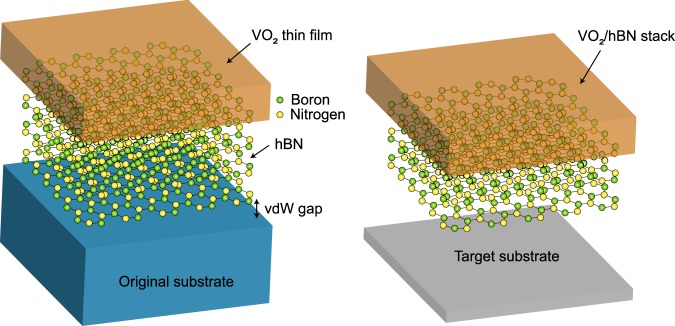
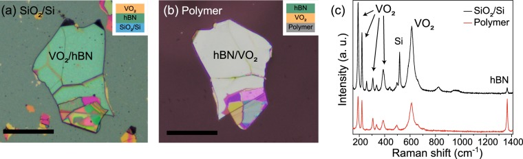
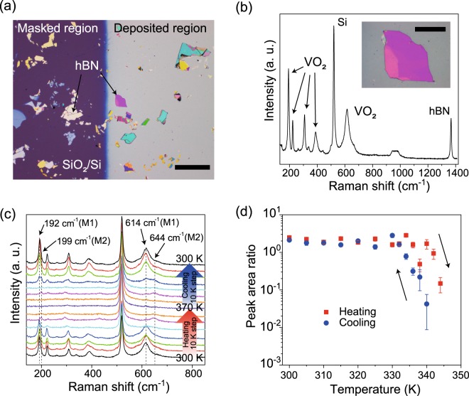
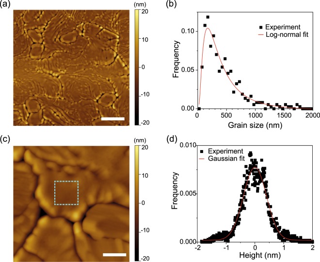
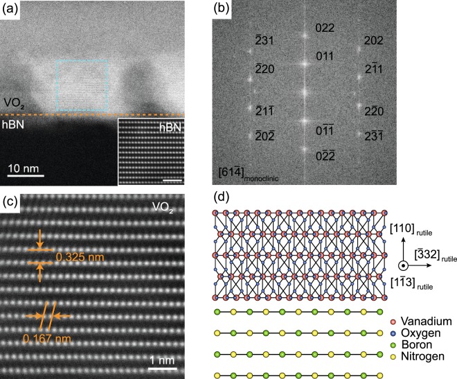
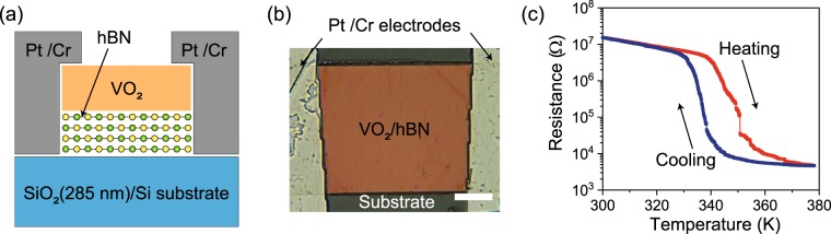
Vanadium dioxide (VO) is an archetypal metal-insulator transition (MIT) material, which has been known for decades to show an orders-of-magnitude change in resistivity across the critical temperature of approximately 340 K. In recent years, VO has attracted increasing interest for electronic and photonic applications, along with advancement in thin film growth techniques. Previously, thin films of VO were commonly grown on rigid substrates such as crystalline oxides and bulk semiconductors, but the use of transferrable materials as the growth substrates can provide versatility in applications, including transparent and flexible devices. Here, we employ single-crystalline hexagonal boron nitride (hBN), which is an insulating layered material, as a substrate for VO thin film growth. VO thin films in the polycrystalline form are grown onto hBN thin flakes exfoliated onto silicon (Si) with a thermal oxide, with grains reaching up-to a micrometer in size. The VO grains on hBN are orientated preferentially with the (110) surface of the rutile structure, which is the most energetically favorable. The VO film on hBN shows a MIT at approximately 340 K, across which the resistivity changes by nearly three orders of magnitude, comparable to VO films grown on common substrates such as sapphire and titanium dioxide. The VO/hBN stack can be picked up from the supporting Si and transferred onto arbitrary substrates, onto which VO thin films cannot be grown directly. Our results pave the way for new possibilities for practical and versatile applications of VO thin films in electronics and photonics.

摘要

二氧化钒(VO)是一种典型的金属-绝缘体转变(MIT)材料,几十年来人们一直知道它在约340K的临界温度下电阻率会发生几个数量级的变化。近年来,随着薄膜生长技术的进步,VO在电子和光子应用方面引起了越来越多的关注。以前,VO薄膜通常生长在刚性衬底上,如晶体氧化物和块状半导体,但使用可转移材料作为生长衬底可以在包括透明和柔性器件在内的应用中提供多功能性。在这里,我们采用单晶六方氮化硼(hBN),一种绝缘层状材料,作为VO薄膜生长的衬底。多晶形式的VO薄膜生长在剥离到带有热氧化物的硅(Si)上的hBN薄片上,晶粒尺寸可达微米级。hBN上的VO晶粒优先以金红石结构的(110)面取向,这是能量上最有利的。hBN上的VO薄膜在约340K时显示出MIT,在此温度范围内电阻率变化近三个数量级,与生长在蓝宝石和二氧化钛等常见衬底上的VO薄膜相当。VO/hBN堆叠可以从支撑硅上取下并转移到任意衬底上,而VO薄膜不能直接生长在这些衬底上。我们的结果为VO薄膜在电子和光子学中的实际和多功能应用开辟了新的可能性。

https://cdn.ncbi.nlm.nih.gov/pmc/blobs/55e2/6393539/1cf4b7cef28d/41598_2019_39091_Fig6_HTML.jpg
https://cdn.ncbi.nlm.nih.gov/pmc/blobs/55e2/6393539/bbfdc1357a35/41598_2019_39091_Fig1_HTML.jpg
https://cdn.ncbi.nlm.nih.gov/pmc/blobs/55e2/6393539/9419231ec878/41598_2019_39091_Fig2_HTML.jpg
https://cdn.ncbi.nlm.nih.gov/pmc/blobs/55e2/6393539/86710dd5f3eb/41598_2019_39091_Fig3_HTML.jpg
https://cdn.ncbi.nlm.nih.gov/pmc/blobs/55e2/6393539/74dc28994829/41598_2019_39091_Fig4_HTML.jpg
https://cdn.ncbi.nlm.nih.gov/pmc/blobs/55e2/6393539/4042810efb6b/41598_2019_39091_Fig5_HTML.jpg
https://cdn.ncbi.nlm.nih.gov/pmc/blobs/55e2/6393539/1cf4b7cef28d/41598_2019_39091_Fig6_HTML.jpg

相似文献

1
Growth of vanadium dioxide thin films on hexagonal boron nitride flakes as transferrable substrates.二氧化钒薄膜在六方氮化硼薄片上的生长作为可转移衬底。
Sci Rep. 2019 Feb 27;9(1):2857. doi: 10.1038/s41598-019-39091-8.
2
Van der Waals Bound Organic/2D Insulator Hybrid Structures: Epitaxial Growth of Acene Films on BN(001) and the Influence of Surface Defects.范德华力束缚的有机/二维绝缘体混合结构:并苯薄膜在BN(001)上的外延生长及表面缺陷的影响。
ACS Appl Mater Interfaces. 2020 Aug 26;12(34):38757-38767. doi: 10.1021/acsami.0c09527. Epub 2020 Aug 12.
3
Gate-Tunable Thermal Metal-Insulator Transition in VO Monolithically Integrated into a WSe Field-Effect Transistor.单片集成到WSe场效应晶体管中的VO中的栅极可调热金属-绝缘体转变
ACS Appl Mater Interfaces. 2019 Jan 23;11(3):3224-3230. doi: 10.1021/acsami.8b18745. Epub 2019 Jan 11.
4
Nanoscale axial position and orientation measurement of hexagonal boron nitride quantum emitters using a tunable nanophotonic environment.利用可调谐纳米光子环境对六方氮化硼量子发射器进行纳米级轴向位置和取向测量。
Nanotechnology. 2021 Oct 20;33(1). doi: 10.1088/1361-6528/ac2b71.
5
Recent Advances in Fabrication of Flexible, Thermochromic Vanadium Dioxide Films for Smart Windows.用于智能窗户的柔性热致变色二氧化钒薄膜制备的最新进展
Nanomaterials (Basel). 2021 Oct 11;11(10):2674. doi: 10.3390/nano11102674.
6
Enhanced Metal-Insulator Transition in Freestanding VO Down to 5 nm Thickness.在厚度低至5纳米的独立式VO₂中增强的金属-绝缘体转变
ACS Appl Mater Interfaces. 2021 Apr 14;13(14):16688-16693. doi: 10.1021/acsami.1c01581. Epub 2021 Apr 1.
7
Stamped production of single-crystal hexagonal boron nitride monolayers on various insulating substrates.在各种绝缘衬底上压印生产单晶六方氮化硼单层。
Nat Commun. 2023 Oct 12;14(1):6421. doi: 10.1038/s41467-023-42270-x.
8
Synthesis of centimeter-scale high-quality polycrystalline hexagonal boron nitride films from Fe fluxes.通过铁助熔剂合成厘米级高质量多晶六方氮化硼薄膜。
Nanoscale. 2021 Jul 1;13(25):11223-11231. doi: 10.1039/d1nr02408f.
9
Ultrathin Films of VO2 on r-Cut Sapphire Achieved by Postdeposition Etching.通过后沉积刻蚀在 r 切蓝宝石上获得 VO2 的超薄薄膜。
ACS Appl Mater Interfaces. 2016 Jun 15;8(23):14863-70. doi: 10.1021/acsami.6b02859. Epub 2016 May 31.
10
Electro-thermal control of aluminum-doped zinc oxide/vanadium dioxide multilayered thin films for smart-device applications.用于智能设备应用的铝掺杂氧化锌/二氧化钒多层薄膜的电热控制
Sci Rep. 2016 Feb 17;6:21040. doi: 10.1038/srep21040.

引用本文的文献

1
Femtosecond-resolved imaging of a single-particle phase transition in energy-filtered ultrafast electron microscopy.飞秒分辨能量过滤超快电子显微镜中单粒子相变的成像。
Sci Adv. 2023 Jan 27;9(4):eadd5375. doi: 10.1126/sciadv.add5375.
2
Surface etching and edge control of hexagonal boron nitride assisted by triangular Sn nanoplates.三角形锡纳米片辅助的六方氮化硼表面蚀刻与边缘控制
Nanoscale Adv. 2022 Aug 8;4(18):3786-3792. doi: 10.1039/d2na00479h. eCollection 2022 Sep 13.
3
Unveiling the optical parameters of vanadium dioxide in the phase transition region: a hybrid modeling approach.

本文引用的文献

1
Reconfigurable infrared hyperbolic metasurfaces using phase change materials.基于相变材料的可重构太赫兹超构表面
Nat Commun. 2018 Oct 22;9(1):4371. doi: 10.1038/s41467-018-06858-y.
2
Capillary-Force-Assisted Clean-Stamp Transfer of Two-Dimensional Materials.基于毛细作用力辅助的二维材料清洁压印转移
Nano Lett. 2017 Nov 8;17(11):6961-6967. doi: 10.1021/acs.nanolett.7b03449. Epub 2017 Oct 27.
3
Mechanical properties of atomically thin boron nitride and the role of interlayer interactions.原子层状氮化硼的力学性能及层间相互作用的作用。
揭示二氧化钒在相变区域的光学参数:一种混合建模方法。
RSC Adv. 2020 Aug 13;10(50):29945-29955. doi: 10.1039/d0ra05890d. eCollection 2020 Aug 10.
Nat Commun. 2017 Jun 22;8:15815. doi: 10.1038/ncomms15815.
4
Wafer-scale growth of VO2 thin films using a combinatorial approach.采用组合方法实现二氧化钒薄膜的晶圆级生长。
Nat Commun. 2015 Oct 9;6:8475. doi: 10.1038/ncomms9475.
5
Strong oxidation resistance of atomically thin boron nitride nanosheets.原子层状氮化硼纳米片具有很强的抗氧化性。
ACS Nano. 2014 Feb 25;8(2):1457-62. doi: 10.1021/nn500059s. Epub 2014 Jan 10.
6
Flexible thermochromic window based on hybridized VO2/graphene.基于混合 VO2/石墨烯的柔性热致变色窗。
ACS Nano. 2013 Jul 23;7(7):5769-76. doi: 10.1021/nn400358x. Epub 2013 Jun 18.
7
Enhanced optical response of hybridized VO₂/graphene films.杂交 VO₂/石墨烯薄膜的增强光学响应。
Nanoscale. 2013 Apr 7;5(7):2632-6. doi: 10.1039/c3nr34054f.
8
Doping-based stabilization of the M2 phase in free-standing VO₂ nanostructures at room temperature.室温下自由-standing VO₂ 纳米结构中基于掺杂的 M2 相稳定化。
Nano Lett. 2012 Dec 12;12(12):6198-205. doi: 10.1021/nl303065h. Epub 2012 Nov 14.
9
Density functional theory study of rutile VO2 surfaces.锐钛矿 VO2 表面的密度泛函理论研究。
J Chem Phys. 2012 Oct 21;137(15):154706. doi: 10.1063/1.4758319.
10
Effective cleaning of hexagonal boron nitride for graphene devices.六方氮化硼的有效清洁及其在石墨烯器件中的应用。
Nano Lett. 2012 Sep 12;12(9):4449-54. doi: 10.1021/nl3011726. Epub 2012 Aug 20.