Zheng Weihao, Zheng Biyuan, Yan Changlin, Liu Ying, Sun Xingxia, Qi Zhaoyang, Yang Tiefeng, Jiang Ying, Huang Wei, Fan Peng, Jiang Feng, Ji Wei, Wang Xiao, Pan Anlian
Key Laboratory for Micro-Nano Physics and Technology of Hunan Province State Key Laboratory of Chemo/Biosensing and Chemometrics and College of Materials Science and Engineering Hunan University Changsha Hunan 410012 China.
Beijing Key Laboratory of Optoelectronic Functional Material & Micro-Nano Devices Department of Physics Renmin University of China Beijing 100872 China.
Adv Sci (Weinh). 2019 Feb 14;6(7):1802204. doi: 10.1002/advs.201802204. eCollection 2019 Apr 3.
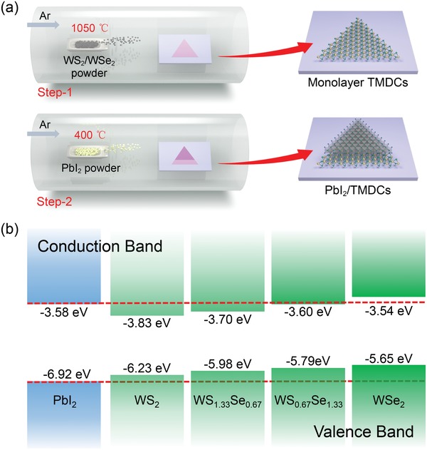
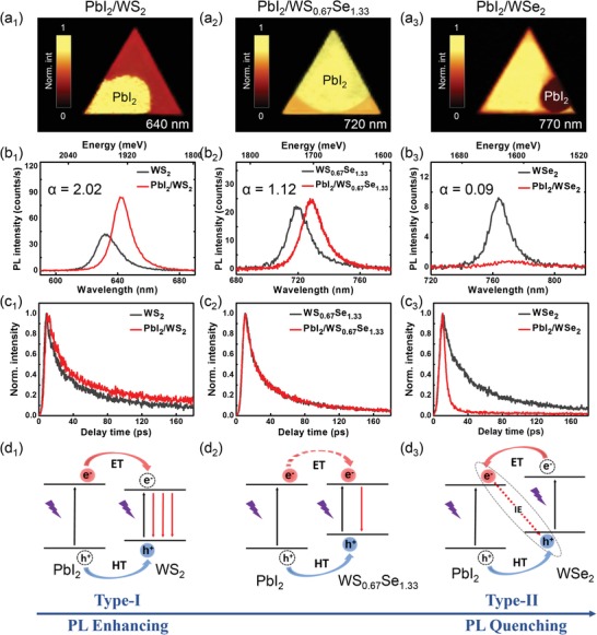
2D vertical van der Waals (vdW) heterostructures with atomically sharp interfaces have attracted tremendous interest in 2D photonic and optoelectronic applications. Band alignment engineering in 2D heterostructures provides a perfect platform for tailoring interfacial charge transfer behaviors, from which desired optical and optoelectronic features can be realized. Here, by developing a two-step chemical vapor deposition strategy, direct vapor growth of monolayer PbI on monolayer transition metal dichalcogenides (TMDCs) (WS, WSe, or alloying WS Se ), forming bilayer vertical heterostructures, is demonstrated. Based on the calculated electron band structures, the interfacial band alignments of the obtained heterostructures can be gradually tuned from type-I (PbI/WS) to type-II (PbI/WSe). Steady-state photoluminescence (PL) and time-resolved PL measurements reveal that the PL emissions from the bottom TMDC layers can be modulated from apparently enhanced (for WS) to greatly quenched (for WSe) compared to their monolayer counterparts, which can be attributed to the band alignment-induced distinct interfacial charge transfer behaviors. The band alignment nature of the heterostructures is further demonstrated by the PL excitation spectroscopy and interlayer exciton investigation. The realization of 2D vertical heterostructures with tunable band alignments will provide a new material platform for designing and constructing multifunctional optoelectronic devices.
具有原子级清晰界面的二维垂直范德华(vdW)异质结构在二维光子和光电子应用中引起了极大的关注。二维异质结构中的能带排列工程为定制界面电荷转移行为提供了一个完美的平台,从中可以实现所需的光学和光电子特性。在此,通过开发一种两步化学气相沉积策略,展示了在单层过渡金属二硫属化物(TMDCs)(WS、WSe或合金化的WS Se )上直接气相生长单层PbI,形成双层垂直异质结构。基于计算得到的电子能带结构,所获得的异质结构的界面能带排列可以从I型(PbI/WS)逐渐调整为II型(PbI/WSe)。稳态光致发光(PL)和时间分辨PL测量表明,与它们的单层对应物相比,底部TMDC层的PL发射可以从明显增强(对于WS)调制到大幅猝灭(对于WSe),这可归因于能带排列引起的不同界面电荷转移行为。PL激发光谱和层间激子研究进一步证明了异质结构的能带排列性质。具有可调能带排列的二维垂直异质结构的实现将为设计和构建多功能光电器件提供一个新的材料平台。