Engineering Research Center for Semiconductor Integrated Technology, Institute of Semiconductors, Chinese Academy of Sciences, Beijing 100083, China.
The School of microelectronics & Center of Materials Science and Optoelectronics Engineering, University of Chinese Academy of Sciences, Beijing 100049, China.
Sensors (Basel). 2020 Jan 7;20(2):337. doi: 10.3390/s20020337.
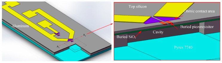
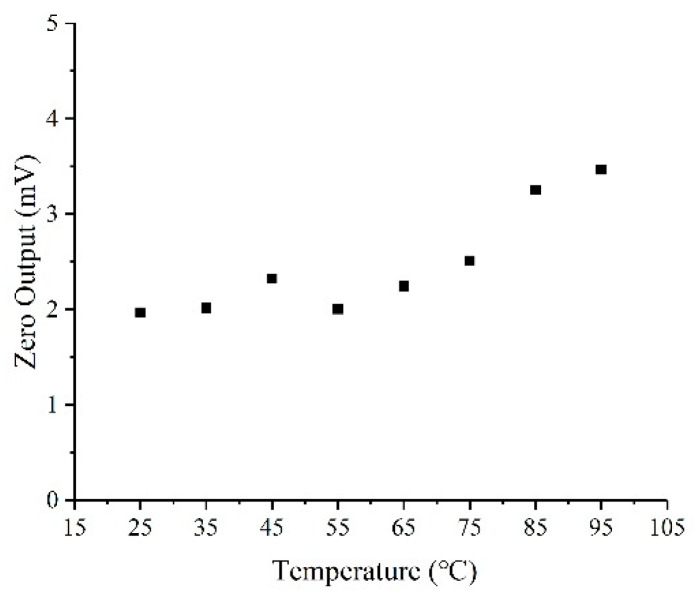
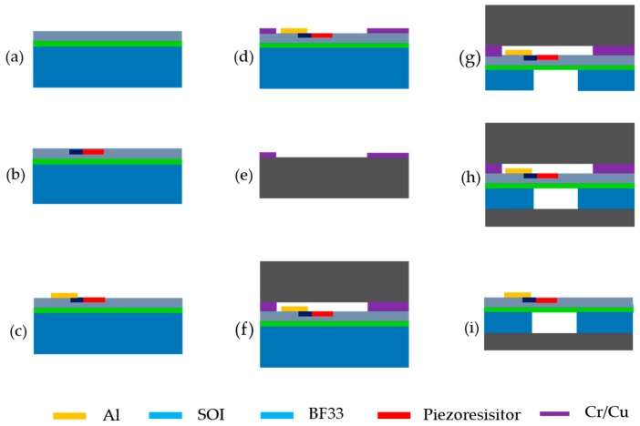
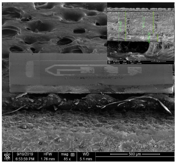
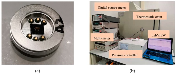
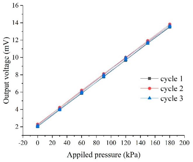
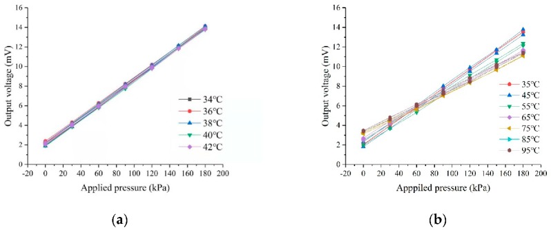
A miniature piezoresistive pressure sensor fabricated by temporary bonding technology was reported in this paper. The sensing membrane was formed on the device layer of an SOI (Silicon-On-Insulator) wafer, which was bonded to borosilicate glass (Borofloat 33, BF33) wafer for supporting before releasing with Cu-Cu bonding after boron doping and electrode patterning. The handle layer was bonded to another BF33 wafer after thinning and etching. Finally, the substrate BF33 wafer was thinned by chemical mechanical polishing (CMP) to reduce the total device thickness. The copper temporary bonding layer was removed by acid solution after dicing to release the sensing membrane. The chip area of the fabricated pressure sensor was of 1600 μm × 650 μm × 104 μm, and the size of a sensing membrane was of 100 μm × 100 μm × 2 μm. A higher sensitivity of 36 μV/(V∙kPa) in the range of 0-180 kPa was obtained. By further reducing the width, the fabricated miniature pressure sensor could be easily mounted in a medical catheter for the blood pressure measurement.
本文报道了一种采用临时键合技术制造的微型压阻压力传感器。传感膜形成在 SOI(绝缘体上硅)晶圆的器件层上,在硼掺杂和电极图案化后,通过 Cu-Cu 键合释放前,先将其键合到硼硅酸盐玻璃(Borofloat 33,BF33)晶圆上以进行支撑。在减薄和刻蚀后,将处理层键合到另一个 BF33 晶圆上。最后,通过化学机械抛光(CMP)将基底 BF33 晶圆减薄,以减小器件总厚度。在切割后,用酸溶液去除铜临时键合层以释放传感膜。所制造的压力传感器的芯片面积为 1600μm×650μm×104μm,传感膜的尺寸为 100μm×100μm×2μm。在 0-180kPa 的范围内,获得了 36μV/(V·kPa)的更高灵敏度。通过进一步减小宽度,所制造的微型压力传感器可以轻松安装在医疗导管中用于血压测量。