Seok Hae-Jun, Kang Yong-Jin, Kim Jongkuk, Kim Do-Hyeong, Heo Su Been, Kang Seong Jun, Kim Han-Ki
School of Advanced Materials Science and Engineering, Sungkyunkwan University, Suwon-si, Republic of Korea.
Surface Engineering Department, Implementation Research Division, Korea Institute of Materials Science (KIMS), Changwon-Si, Republic of Korea.
Sci Technol Adv Mater. 2019 Nov 22;20(1):1118-1130. doi: 10.1080/14686996.2019.1694841. eCollection 2019.
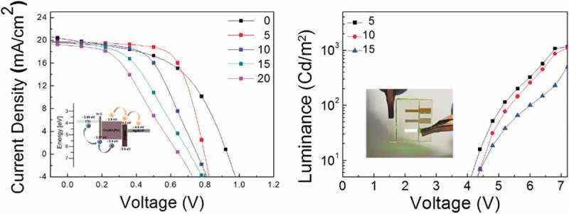
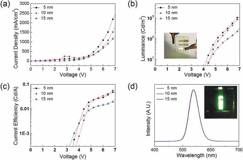
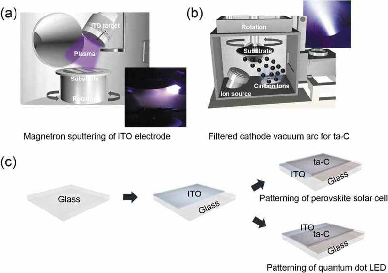
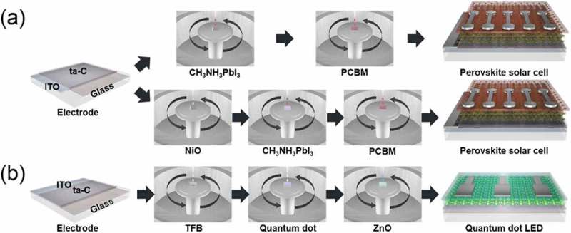
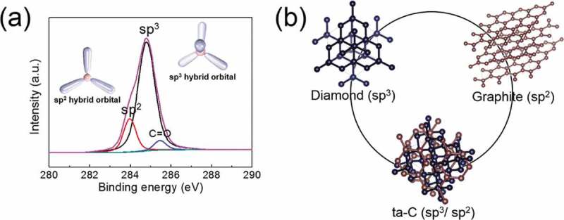
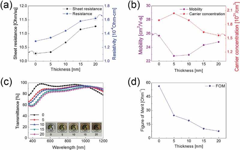
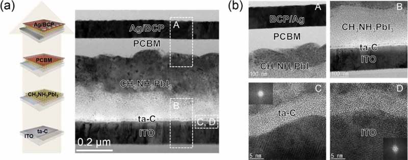
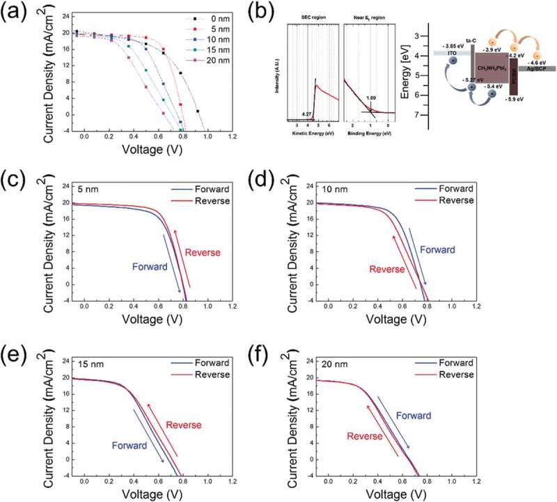
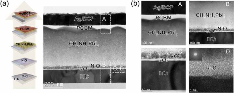
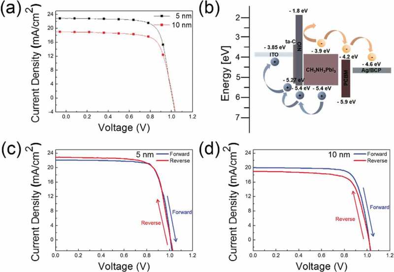
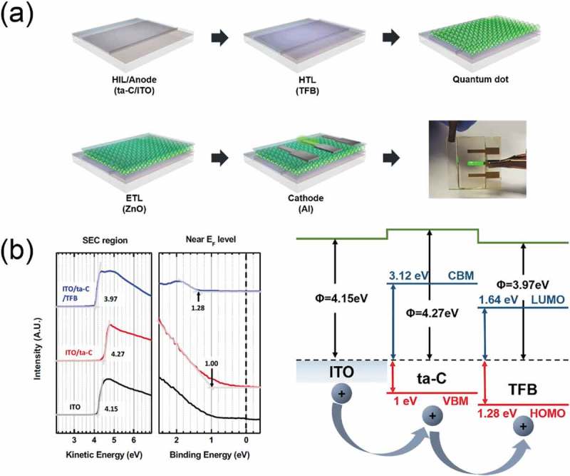
(ta-C) films coated through the filtered cathodic vacuum arc (FCVA) process as a hole transport layer (HTL) for perovskite solar cells (PSCs) and quantum dot light-emitting diodes (QDLEDs). The p-type ta-C film has several remarkable features, including ease of fabrication without the need for thermal annealing, reasonable electrical conductivity, optical transmittance, and a high work function. X-ray photoelectron spectroscopy and ultraviolet photoelectron spectroscopy examinations show that the electrical properties (sp/sp hybridized bond) and work function of the ta-C HTL are appropriate for PSCs and QDLEDs. In addition, in order to correlate the performance of the devices, the optical, surface morphological, and structural properties of the FCVA-grown ta-C films with different thicknesses (5 ~ 20 nm) deposited on the ITO anode are investigated in detail. The optimized ta-C film with a thickness of 5 nm deposited on the ITO anode had a sheet resistance of 10.33 Ω, a resistivity of 1.34 × 10 Ω cm, and an optical transmittance of 88.97%. Compared to the reference PSC with p-NiO HTL, the PSC with 5 nm thick ta-C HTL yielded a higher power conversion efficiency (PCE, 10.53%) due to its improved fill factor. Further, the performance of QDLEDs with 5 nm thick ta-C hole injection layers (HIL) showed better than the performance of QDLEDs with different ta-C thicknesses. It is concluded that ta-C films have the potential to serve as HTL and HIL in next-generation PSCs and QDLEDs.
通过过滤阴极真空电弧(FCVA)工艺制备的(ta-C)薄膜,用作钙钛矿太阳能电池(PSC)和量子点发光二极管(QDLED)的空穴传输层(HTL)。p型ta-C薄膜具有几个显著特性,包括易于制备且无需热退火、合理的电导率、光学透过率和高功函数。X射线光电子能谱和紫外光电子能谱检测表明,ta-C HTL的电学性质(sp/sp杂化键)和功函数适用于PSC和QDLED。此外,为了关联器件的性能,详细研究了沉积在ITO阳极上不同厚度(5~20nm)的FCVA生长的ta-C薄膜的光学、表面形态和结构性质。沉积在ITO阳极上的厚度为5nm的优化ta-C薄膜的方块电阻为10.33Ω,电阻率为1.34×10Ω·cm,光学透过率为88.97%。与具有p-NiO HTL的参考PSC相比,具有5nm厚ta-C HTL的PSC由于其填充因子的提高而产生了更高的功率转换效率(PCE,10.53%)。此外,具有5nm厚ta-C空穴注入层(HIL)的QDLED的性能优于具有不同ta-C厚度的QDLED。得出结论,ta-C薄膜有潜力在下一代PSC和QDLED中用作HTL和HIL。