Department of Mechanical and Materials Engineering, Florida International University, College of Engineering and Computing, Miami, Florida, United States of America.
Institute National de la Recherche Scientifique, Centre Énergie, Matériaux et Télécommunications, Varennes, Québec, Canada.
PLoS One. 2020 May 5;15(5):e0232184. doi: 10.1371/journal.pone.0232184. eCollection 2020.
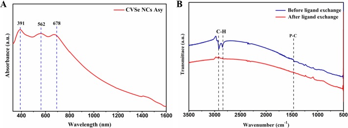
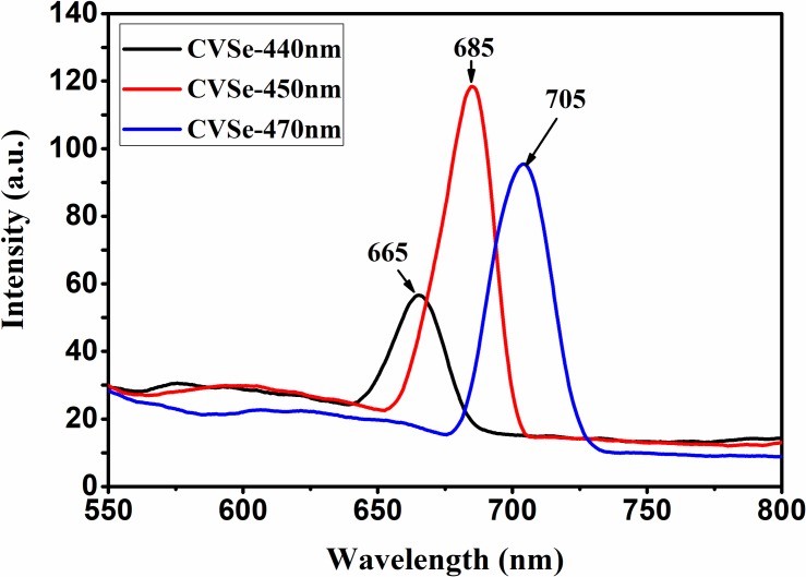
The ternary chalcogenide Cu3VSe4 (CVSe) with sulvanite structure has been theoretically predicted to be a promising candidate for photovoltaic applications due to its suitable bandgap for solar absorption and the relatively earth-abundant elements in its composition. To realize the absorber layer via an inexpensive route, printed thin-films could be fabricated from dispersions of nano-sized Cu3VSe4 precursors. Herein, cubic Cu3VSe4 nanocrystals were successfully synthesized via a hot-injection method. Similar with reported Cu3VS4 nanocrystals, Cu3VSe4 nanocrystals with cubic structure exhibit three absorption bands in the UV-Visible range indicative of a potential intermediate bandgap existence. A thin film fabricated by depositing the nanoparticles Cu3VSe4 on FTO coated glass substrate, exhibited a p-type behavior and a photocurrent of ~ 4 μA/cm2 when measured in an electrochemical cell setting. This first demonstration of photocurrent exhibited by a CVSe nanocrystals thin film signifies a promising potential in photovoltaic applications.
具有硫银矿结构的三元硒化物 Cu3VSe4(CVSe)由于其适合太阳能吸收的能带隙和组成中相对丰富的地球元素,在理论上被预测为一种有前途的光伏应用候选材料。为了通过廉价的途径实现吸收层,可以从纳米级 Cu3VSe4 前体的分散体中制造印刷的薄膜。在此,通过热注入法成功合成了立方 Cu3VSe4 纳米晶。与报道的 Cu3VS4 纳米晶类似,具有立方结构的 Cu3VSe4 纳米晶在 UV-可见范围内显示出三个吸收带,表明存在潜在的中间能带隙。通过将纳米粒子 Cu3VSe4 沉积在 FTO 涂覆的玻璃基底上制成的薄膜,在电化学池设置中测量时表现出 p 型行为和约 4 μA/cm2 的光电流。这种由 CVSe 纳米晶薄膜表现出的光电流的首次演示表明了在光伏应用中具有有前途的潜力。