Choi Sukyung, Kang Chan-Mo, Byun Chun-Won, Cho Hyunsu, Kwon Byoung-Hwa, Han Jun-Han, Yang Jong-Heon, Shin Jin-Wook, Hwang Chi-Sun, Cho Nam Sung, Lee Kang Me, Kim Hee-Ok, Kim Eungjun, Yoo Seunghyup, Lee Hyunkoo
Reality Display Research Section, Electronics and Telecommunications Research Institute (ETRI), Daejeon, 34129, Republic of Korea.
School of Electrical Engineering, Korea Advanced Institute of Science and Technology (KAIST), Daejeon, 34141, Republic of Korea.
Nat Commun. 2020 Jun 1;11(1):2732. doi: 10.1038/s41467-020-16551-8.
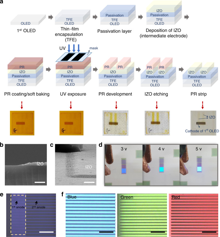
Thin-film transistor (TFT)-driven full-color organic light-emitting diodes (OLEDs) with vertically stacked structures are developed herein using photolithography processes, which allow for high-resolution displays of over 2,000 pixels per inch. Vertical stacking of OLEDs by the photolithography process is technically challenging, as OLEDs are vulnerable to moisture, oxygen, solutions for photolithography processes, and temperatures over 100 °C. In this study, we develop a low-temperature processed AlO/SiN bilayered protection layer, which stably protects the OLEDs from photolithography process solutions, as well as from moisture and oxygen. As a result, transparent intermediate electrodes are patterned on top of the OLED elements without degrading the OLED, thereby enabling to fabricate the vertically stacked OLED. The aperture ratio of the full-color-driven OLED pixel is approximately twice as large as conventional sub-pixel structures, due to geometric advantage, despite the TFT integration. To the best of our knowledge, we first demonstrate the TFT-driven vertically stacked full-color OLED.
本文采用光刻工艺开发了具有垂直堆叠结构的薄膜晶体管(TFT)驱动的全彩色有机发光二极管(OLED),该工艺可实现每英寸超过2000像素的高分辨率显示。通过光刻工艺对OLED进行垂直堆叠在技术上具有挑战性,因为OLED易受湿气、氧气、光刻工艺溶液以及超过100°C的温度影响。在本研究中,我们开发了一种低温处理的AlO/SiN双层保护层,该保护层可稳定地保护OLED免受光刻工艺溶液以及湿气和氧气的影响。结果,透明中间电极可以在OLED元件顶部进行图案化,而不会使OLED性能下降,从而能够制造垂直堆叠的OLED。尽管集成了TFT,但由于几何优势,全彩色驱动OLED像素的开口率约为传统子像素结构的两倍。据我们所知,我们首次展示了TFT驱动的垂直堆叠全彩色OLED。