Mall Abhishek, Patil Abhijeet, Sethi Amit, Kumar Anshuman
Department of Physics, Indian Institute of Technology - Bombay, Mumbai, 400076, India.
Department of Electrical Engineering, Indian Institute of Technology - Bombay, Mumbai, 400076, India.
Sci Rep. 2020 Nov 10;10(1):19427. doi: 10.1038/s41598-020-76400-y.
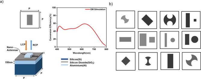
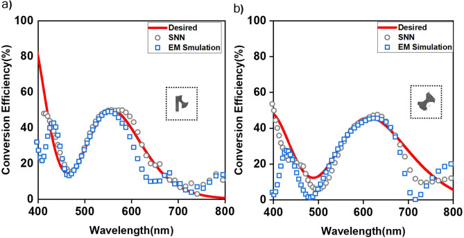
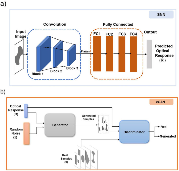
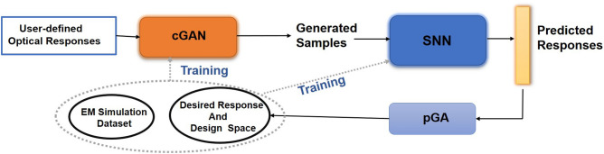
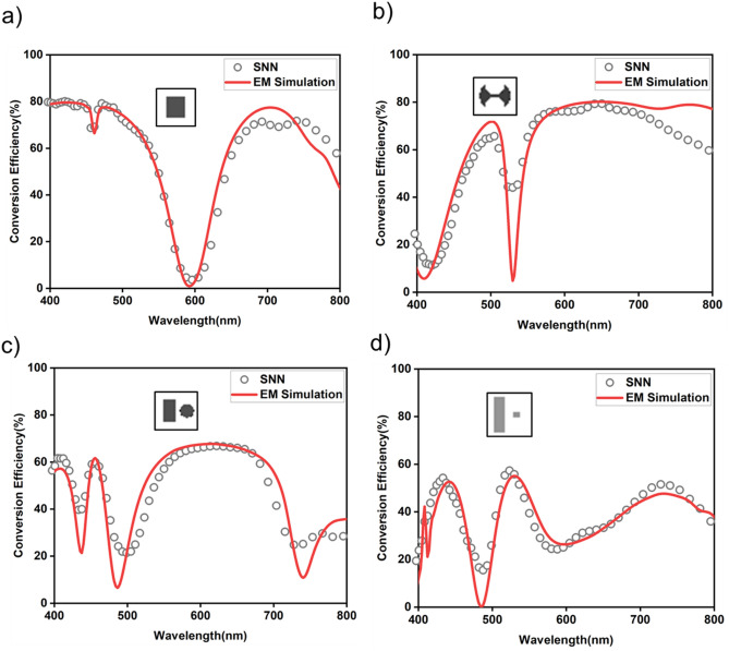
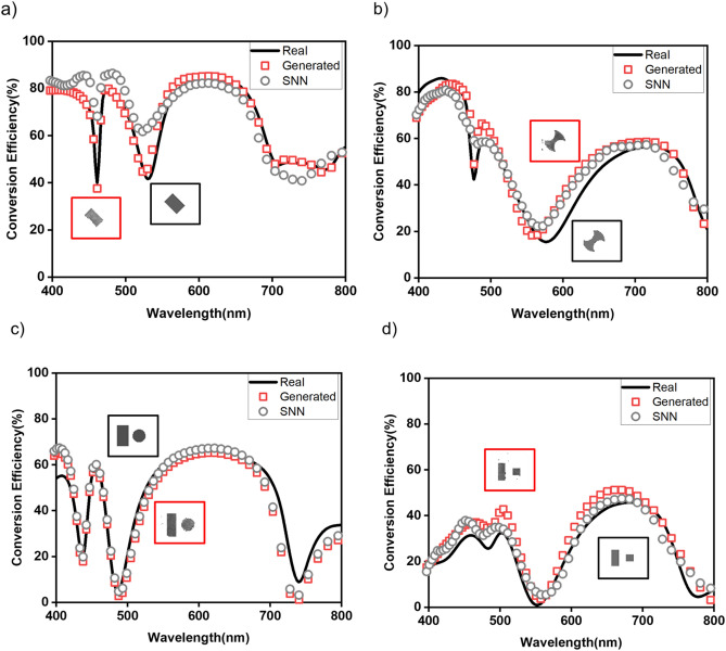
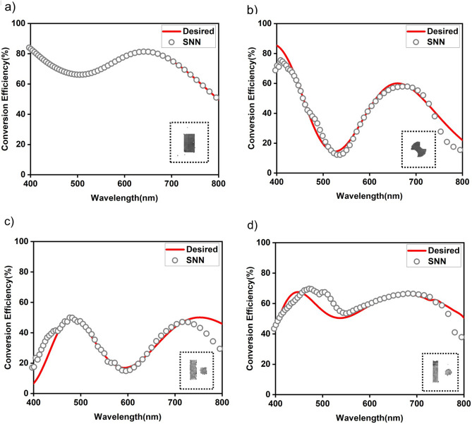
The conventional approach to nanophotonic metasurface design and optimization for a targeted electromagnetic response involves exploring large geometry and material spaces. This is a highly iterative process based on trial and error, which is computationally costly and time consuming. Moreover, the non-uniqueness of structural designs and high non-linearity between electromagnetic response and design makes this problem challenging. To model this unintuitive relationship between electromagnetic response and metasurface structural design as a probability distribution in the design space, we introduce a framework for inverse design of nanophotonic metasurfaces based on cyclical deep learning (DL). The proposed framework performs inverse design and optimization mechanism for the generation of meta-atoms and meta-molecules as metasurface units based on DL models and genetic algorithm. The framework includes consecutive DL models that emulate both numerical electromagnetic simulation and iterative processes of optimization, and generate optimized structural designs while simultaneously performing forward and inverse design tasks. A selection and evaluation of generated structural designs is performed by the genetic algorithm to construct a desired optical response and design space that mimics real world responses. Importantly, our cyclical generation framework also explores the space of new metasurface topologies. As an example application of the utility of our proposed architecture, we demonstrate the inverse design of gap-plasmon based half-wave plate metasurface for user-defined optical response. Our proposed technique can be easily generalized for designing nanophtonic metasurfaces for a wide range of targeted optical response.
用于实现目标电磁响应的纳米光子超表面设计与优化的传统方法,涉及探索庞大的几何结构和材料空间。这是一个基于反复试验的高度迭代过程,计算成本高昂且耗时。此外,结构设计的非唯一性以及电磁响应与设计之间的高度非线性,使得这个问题具有挑战性。为了将电磁响应与超表面结构设计之间这种不直观的关系建模为设计空间中的概率分布,我们引入了一种基于循环深度学习(DL)的纳米光子超表面逆向设计框架。所提出的框架基于DL模型和遗传算法,执行逆向设计和优化机制,以生成作为超表面单元的元原子和元分子。该框架包括连续的DL模型,这些模型模拟数值电磁仿真和优化的迭代过程,并在执行正向和逆向设计任务的同时生成优化的结构设计。通过遗传算法对生成的结构设计进行选择和评估,以构建模拟真实世界响应的所需光学响应和设计空间。重要的是,我们的循环生成框架还探索了新的超表面拓扑结构空间。作为我们所提出架构实用性的一个示例应用,我们展示了基于间隙等离子体的半波片超表面针对用户定义光学响应的逆向设计。我们提出的技术可以很容易地推广到设计用于广泛目标光学响应的纳米光子超表面。