Chu Shenglong, Chen Wenjing, Fang Zhibin, Xiao Xun, Liu Yan, Chen Jia, Huang Jinsong, Xiao Zhengguo
Hefei National Laboratory for Physical Science at the Microscale, Department of Physics, CAS Key Laboratory of Strongly-Coupled Quantum Matter Physics, University of Science and Technology of China, Hefei, Anhui, 230026, China.
Department of Applied Physical Sciences, University of North Carolina at Chapel Hill, Chapel Hill, NC, 27599, USA.
Nat Commun. 2021 Jan 8;12(1):147. doi: 10.1038/s41467-020-20433-4.
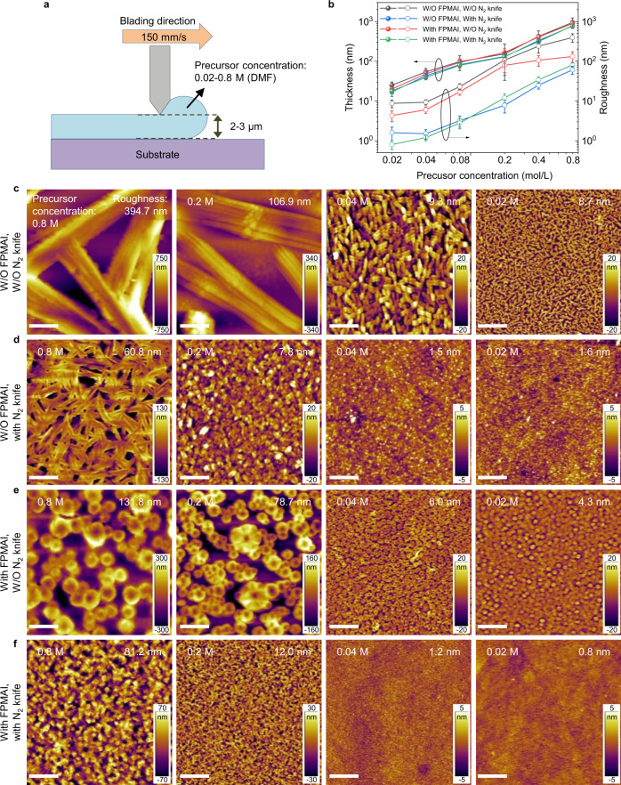
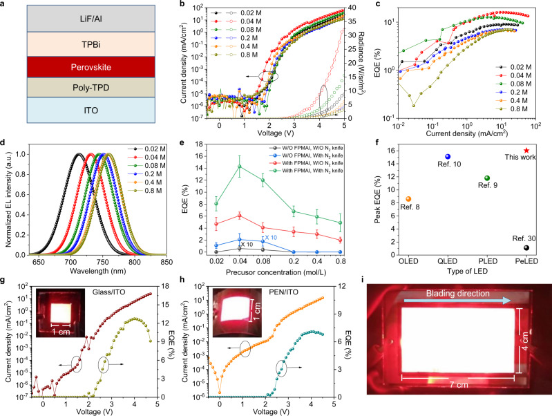
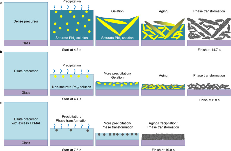
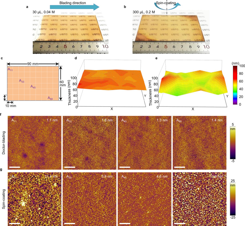
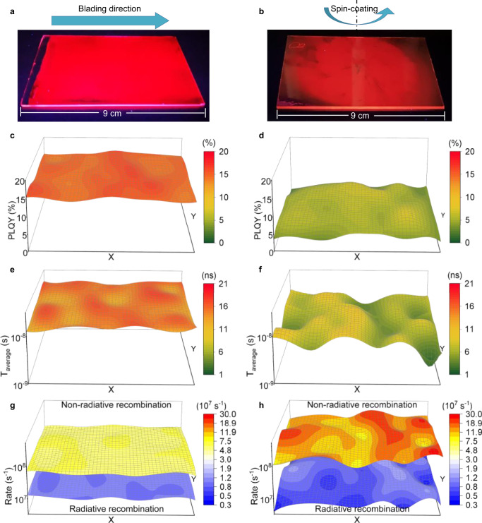
Large-area light-emitting diodes (LEDs) fabricated by mass-production techniques are needed for low-cost flat-panel lighting. Nevertheless, it is still challenging to fabricate efficient large-area LEDs using organic small molecules (OLEDs), quantum dots (QLEDs), polymers (PLEDs), and recently-developed hybrid perovskites (PeLEDs) due to difficulties controlling film uniformity. To that end, we report sol-gel engineering of low-temperature blade-coated methylammonium lead iodide (MAPbI) perovskite films. The precipitation, gelation, aging, and phase transformation stages are dramatically shortened by using a diluted, organoammonium-excessed precursor, resulting in ultra-flat large-area films (54 cm) with roughness reaching 1 nm. The external quantum efficiency of doctor-bladed PeLEDs reaches 16.1%, higher than that of best-performing blade-coated OLEDs, QLEDs, and PLEDs. Furthermore, benefitting from the throughput of the blade-coating process and cheap materials, the expected cost of the emissive layer is projected to be as low as 0.02 cents per cm, emphasizing its application potential.
低成本平板照明需要采用大规模生产技术制造的大面积发光二极管(LED)。然而,由于难以控制薄膜均匀性,使用有机小分子(OLED)、量子点(QLED)、聚合物(PLED)以及最近开发的混合钙钛矿(PeLED)来制造高效大面积LED仍然具有挑战性。为此,我们报道了低温刮刀涂布的甲基碘化铅(MAPbI)钙钛矿薄膜的溶胶-凝胶工程。通过使用稀释的、有机铵过量的前驱体,沉淀、凝胶化、老化和相变阶段被大大缩短,从而得到超平整的大面积薄膜(54厘米),粗糙度达到1纳米。刮刀涂布的PeLED的外量子效率达到16.1%,高于性能最佳的刮刀涂布OLED、QLED和PLED。此外,受益于刮刀涂布工艺的产量和廉价材料,发射层的预期成本预计低至每平方厘米0.02美分,突出了其应用潜力。