Hu Dejiao, Li Hao, Zhu Yupeng, Lei Yuqiu, Han Jing, Xian Shilin, Zheng Jiajin, Guan Bai-Ou, Cao Yaoyu, Bi Lei, Li Xiangping
Guangdong Provincial Key Laboratory of Optical Fiber Sensing and Communications, Institute of Photonics Technology, Jinan University, Guangzhou, China.
National Engineering Research Center of Electromagnetic Radiation Control Materials, University of Electronic Science and Technology of China, Chengdu, China.
Nat Commun. 2021 Feb 19;12(1):1154. doi: 10.1038/s41467-021-21499-4.
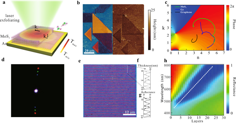
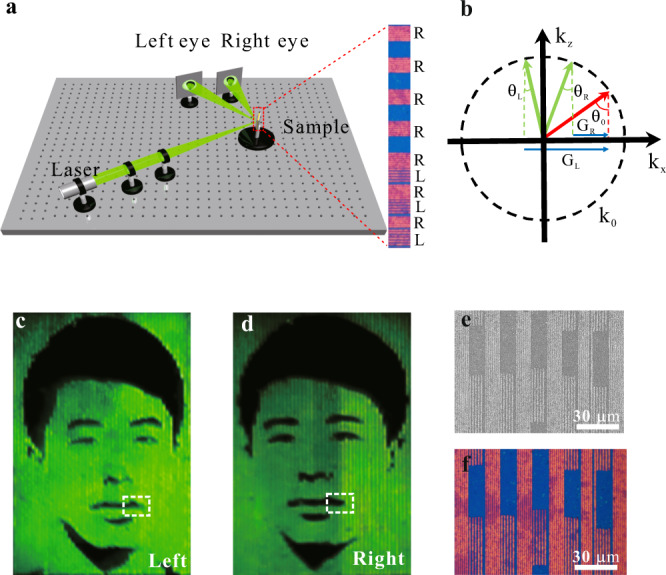
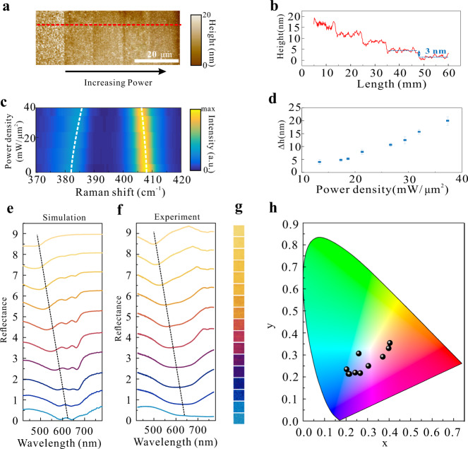
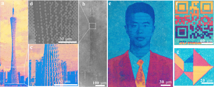
Two-dimensional (2D) transition metal dichalcogenides (TMDs) with tantalizing layer-dependent electronic and optical properties have emerged as a paradigm for integrated flat opto-electronic devices, but their widespread applications are hampered by challenges in deterministic fabrication with demanded shapes and thicknesses, as well as light field manipulation in such atomic-thick layers with negligible thicknesses compared to the wavelength. Here we demonstrate ultra-sensitive light field manipulation in full visible ranges based on MoS laser prints exfoliated with nanometric precisions. The nontrivial interfacial phase shifts stemming from the unique dispersion of MoS layers integrated on the metallic substrate empower an ultra-sensitive resonance manipulation up to 13.95 nm per MoS layer across the entire visible bands, which is up to one-order-of-magnitude larger than their counterparts. The interlayer van der Waals interactions and the anisotropic thermal conductivity of layered MoS films endow a laser exfoliation method for on-demand patterning MoS with atomic thickness precision and subwavelength feature sizes. With this, nanometric flat color prints and further amplitude-modulated diffractive components for binocular stereoscopic images can be realized in a facile and lithography-free fashion. Our results with demonstrated practicality unlock the potentials of, and pave the way for, widespread applications of emerging 2D flat optics.
具有诱人的层依赖电子和光学特性的二维(2D)过渡金属二硫属化物(TMD)已成为集成平面光电器件的范例,但其广泛应用受到具有所需形状和厚度的确定性制造挑战的阻碍,以及在与波长相比厚度可忽略不计的此类原子厚层中的光场操纵的阻碍。在此,我们展示了基于以纳米精度剥落的MoS激光打印在整个可见光范围内的超灵敏光场操纵。源自集成在金属基板上的MoS层的独特色散的非平凡界面相移,在整个可见波段中实现了高达每MoS层13.95 nm的超灵敏共振操纵,这比同类产品大一个数量级。层状MoS薄膜的层间范德华相互作用和各向异性热导率赋予了一种激光剥落方法,可按需对具有原子厚度精度和亚波长特征尺寸的MoS进行图案化。由此,可以以简便且无需光刻的方式实现纳米级平面彩色打印以及用于双目立体图像的进一步幅度调制衍射组件。我们具有实用性的结果释放了新兴二维平面光学的潜力,并为其广泛应用铺平了道路。