Chu Liang, Ahmad Waqar, Liu Wei, Yang Jian, Zhang Rui, Sun Yan, Yang Jianping, Li Xing'ao
New Energy Technology Engineering Laboratory of Jiangsu Province & School of Science, Nanjing University of Posts and Telecommunications (NJUPT), Nanjing, 210023, People's Republic of China.
Key Laboratory for Organic Electronics & Information Displays & Institute of Advanced Materials, Jiangsu National Synergistic Innovation Center for Advanced Materials, School of Materials Science and Engineering, Nanjing University of Posts and Telecommunications (NJUPT), Nanjing, 210023, People's Republic of China.
Nanomicro Lett. 2019 Feb 27;11(1):16. doi: 10.1007/s40820-019-0244-6.
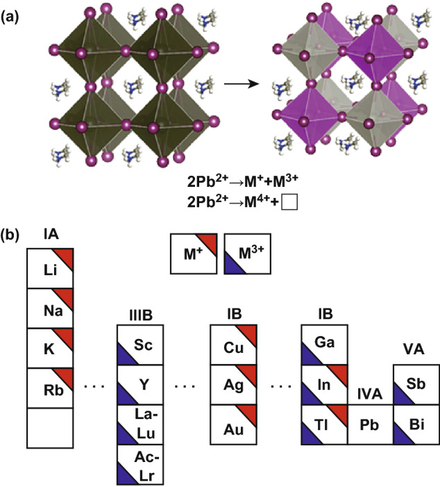
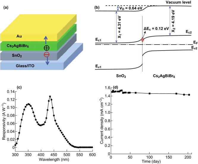
Lead-based halide perovskites have emerged as excellent semiconductors for a broad range of optoelectronic applications, such as photovoltaics, lighting, lasing and photon detection. However, toxicity of lead and poor stability still represent significant challenges. Fortunately, halide double perovskite materials with formula of AM(I)M(III)X or AM(IV)X could be potentially regarded as stable and green alternatives for optoelectronic applications, where two divalent lead ions are substituted by combining one monovalent and one trivalent ions, or one tetravalent ion. Here, the article provides an up-to-date review on the developments of halide double perovskite materials and their related optoelectronic applications including photodetectors, X-ray detectors, photocatalyst, light-emitting diodes and solar cells. The synthesized halide double perovskite materials exhibit exceptional stability, and a few possess superior optoelectronic properties. However, the number of synthesized halide double perovskites is limited, and more limited materials have been developed for optoelectronic applications to date. In addition, the band structures and carrier transport properties of the materials are still not desired, and the films still manifest low quality for photovoltaic applications. Therefore, we propose that continuing efforts are needed to develop more halide double perovskites, modulate the properties and grow high-quality films, with the aim of opening the wild practical applications.
铅基卤化物钙钛矿已成为用于广泛光电子应用的优秀半导体,如光伏、照明、激光和光子探测。然而,铅的毒性和较差的稳定性仍然是重大挑战。幸运的是,化学式为AM(I)M(III)X或AM(IV)X的卤化物双钙钛矿材料有可能被视为光电子应用中稳定且绿色的替代品,其中两个二价铅离子被一个一价离子和一个三价离子或一个四价离子组合取代。在此,本文对卤化物双钙钛矿材料的发展及其相关光电子应用进行了最新综述,包括光电探测器、X射线探测器、光催化剂、发光二极管和太阳能电池。合成的卤化物双钙钛矿材料表现出卓越的稳定性,少数具有优异的光电子性能。然而,合成的卤化物双钙钛矿数量有限,迄今为止用于光电子应用开发的材料更是有限。此外,材料的能带结构和载流子传输特性仍不尽人意,并且这些薄膜在光伏应用中仍表现出低质量。因此,我们建议需要继续努力开发更多的卤化物双钙钛矿,调节其性能并生长高质量薄膜,以期开启广泛的实际应用。