Zhang Minfang, Yang Mei, Okigawa Yuki, Yamada Takatoshi, Nakajima Hideaki, Iizumi Yoko, Okazaki Toshiya
CNT Application Research Center, National Institute of Advanced Industrial Science and Technology (AIST), Higashi 1-1-1, Tsukuba, Japan.
Nanomaterials Research Institute, National Institute of Advanced Industrial Science and Technology (AIST), Higashi 1-1-1, Tsukuba, Japan.
Sci Rep. 2022 Mar 16;12(1):4541. doi: 10.1038/s41598-022-08674-3.
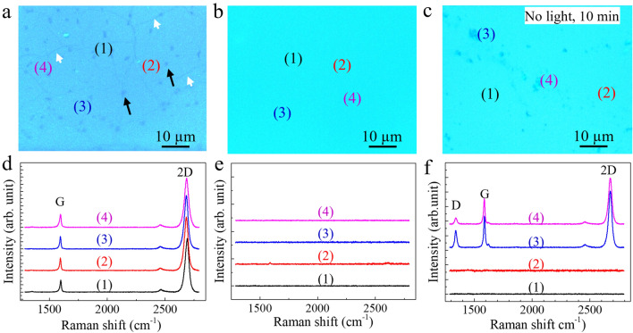
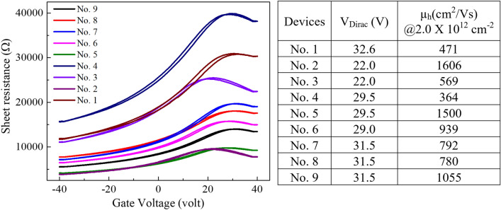
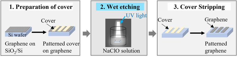
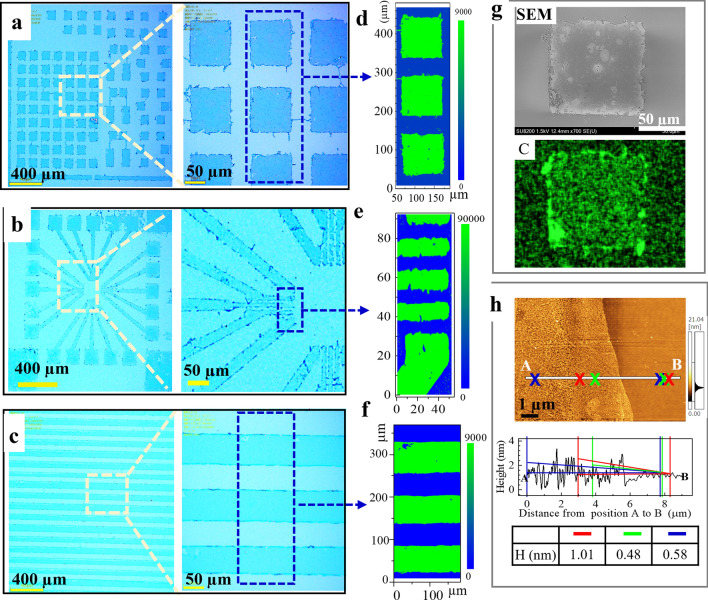
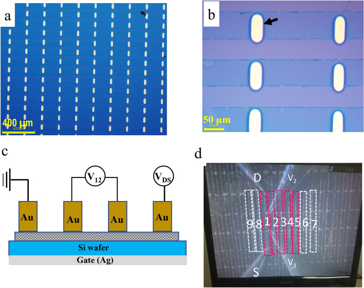
Graphene patterning via etching is important for enhancing or controling the properties of devices and supporting their applications in micro- and nano-electronic fields. Herein, we present a simple, low-cost, and scalable wet etching method for graphene patterning. The technique uses hypochlorite solution combined with ultraviolet light irradiation to rapidly remove unwanted graphene areas from the substrate. Raman spectroscopy, atomic force microscopy, scanning electron microscopy, and optical microscopy results showed that well-patterned graphene with micrometer scale regions was successfully prepared. Furthermore, graphene field effect transistor arrays were fabricated, and the obtained devices exhibited good current-voltage characteristics, with maximum mobility of ~ 1600 cm/Vs, confirming the feasibility of the developed technique.
通过蚀刻进行石墨烯图案化对于增强或控制器件性能以及支持其在微纳电子领域的应用至关重要。在此,我们提出了一种用于石墨烯图案化的简单、低成本且可扩展的湿法蚀刻方法。该技术使用次氯酸盐溶液结合紫外线照射,以快速从基板上去除不需要的石墨烯区域。拉曼光谱、原子力显微镜、扫描电子显微镜和光学显微镜结果表明,成功制备了具有微米级区域的图案良好的石墨烯。此外,制备了石墨烯场效应晶体管阵列,所获得的器件表现出良好的电流 - 电压特性,最大迁移率约为1600 cm²/V·s,证实了所开发技术的可行性。