• 文献检索
  • 文档翻译
  • 深度研究
  • 学术资讯
  • Suppr Zotero 插件Zotero 插件
  • 邀请有礼
  • 套餐&价格
  • 历史记录
应用&插件
Suppr Zotero 插件Zotero 插件浏览器插件Mac 客户端Windows 客户端微信小程序
定价
高级版会员购买积分包购买API积分包
服务
文献检索文档翻译深度研究API 文档MCP 服务
关于我们
关于 Suppr公司介绍联系我们用户协议隐私条款
关注我们

Suppr 超能文献

核心技术专利:CN118964589B侵权必究
粤ICP备2023148730 号-1Suppr @ 2026

文献检索

告别复杂PubMed语法,用中文像聊天一样搜索,搜遍4000万医学文献。AI智能推荐,让科研检索更轻松。

立即免费搜索

文件翻译

保留排版,准确专业,支持PDF/Word/PPT等文件格式,支持 12+语言互译。

免费翻译文档

深度研究

AI帮你快速写综述,25分钟生成高质量综述,智能提取关键信息,辅助科研写作。

立即免费体验

通过NaCl辅助化学气相沉积法合成的亚毫米尺寸高迁移率单晶MoSe单分子层。

Sub-millimeter size high mobility single crystal MoSe monolayers synthesized by NaCl-assisted chemical vapor deposition.

作者信息

Li Juncheng, Yan Wenjie, Lv Yanhui, Leng Jian, Zhang Duan, Ó Coileáin Cormac, Cullen Conor P, Stimpel-Lindner Tanja, Duesberg Georg S, Cho Jiung, Choi Miri, Chun Byong Sun, Zhao Yanfeng, Lv Chengzhai, Arora Sunil K, Wu Han-Chun

机构信息

School of Physics, Beijing Institute of Technology Beijing 100081 P. R. China

Elementary Educational College, Beijing Key Laboratory for Nano-Photonics and Nano-Structure, Capital Normal University Beijing 100048 P. R. China.

出版信息

RSC Adv. 2020 Jan 8;10(3):1580-1587. doi: 10.1039/c9ra09103c. eCollection 2020 Jan 7.

DOI:10.1039/c9ra09103c
PMID:35494696
原文链接:https://pmc.ncbi.nlm.nih.gov/articles/PMC9048230/
Abstract

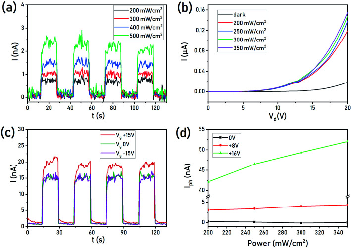
Monolayer MoSe is a transition metal dichalcogenide with a narrow bandgap, high optical absorbance and large spin-splitting energy, giving it great promise for applications in the field of optoelectronics. Producing monolayer MoSe films in a reliable and scalable manner is still a challenging task as conventional chemical vapor deposition (CVD) or exfoliation based techniques are limited due to the small domains/nanosheet sizes obtained. Here, based on NaCl assisted CVD, we demonstrate the simple and stable synthesis of sub-millimeter size single-crystal MoSe monolayers with mobilities ranging from 38 to 8 cm V s. The average mobility is 12 cm V s. We further determine that the optical responsivity of monolayer MoSe is 42 mA W, with an external quantum efficiency of 8.22%.

摘要

单层二硒化钼是一种具有窄带隙、高光学吸收率和大自旋分裂能的过渡金属二卤化物,这使其在光电子领域具有广阔的应用前景。以可靠且可扩展的方式制备单层二硒化钼薄膜仍然是一项具有挑战性的任务,因为传统的化学气相沉积(CVD)或基于剥离的技术由于所获得的小畴/纳米片尺寸而受到限制。在此,基于氯化钠辅助的CVD,我们展示了简单且稳定地合成亚毫米尺寸的单晶单层二硒化钼,其迁移率范围为38至8 cm V s。平均迁移率为12 cm V s。我们进一步确定单层二硒化钼的光学响应率为42 mA W,外部量子效率为8.22%。

https://cdn.ncbi.nlm.nih.gov/pmc/blobs/0616/9048230/9ed50b37323c/c9ra09103c-f4.jpg
https://cdn.ncbi.nlm.nih.gov/pmc/blobs/0616/9048230/c50feb4cf9ff/c9ra09103c-f1.jpg
https://cdn.ncbi.nlm.nih.gov/pmc/blobs/0616/9048230/b5d6224f199d/c9ra09103c-f2.jpg
https://cdn.ncbi.nlm.nih.gov/pmc/blobs/0616/9048230/0d3e54d8ea01/c9ra09103c-f3.jpg
https://cdn.ncbi.nlm.nih.gov/pmc/blobs/0616/9048230/9ed50b37323c/c9ra09103c-f4.jpg

相似文献

1
Sub-millimeter size high mobility single crystal MoSe monolayers synthesized by NaCl-assisted chemical vapor deposition.通过NaCl辅助化学气相沉积法合成的亚毫米尺寸高迁移率单晶MoSe单分子层。
RSC Adv. 2020 Jan 8;10(3):1580-1587. doi: 10.1039/c9ra09103c. eCollection 2020 Jan 7.
2
Chemical vapor deposition growth of crystalline monolayer MoSe2.化学气相沉积法生长单晶层 MoSe2。
ACS Nano. 2014 May 27;8(5):5125-31. doi: 10.1021/nn501175k. Epub 2014 Apr 8.
3
Chemical Vapor Deposition of Large-Size Monolayer MoSe Crystals on Molten Glass.在熔融玻璃上化学气相沉积大面积单层 MoSe 晶体。
J Am Chem Soc. 2017 Jan 25;139(3):1073-1076. doi: 10.1021/jacs.6b12156. Epub 2017 Jan 10.
4
Boosting Monolayer Transition Metal Dichalcogenides Growth by Hydrogen-Free Ramping during Chemical Vapor Deposition.在化学气相沉积过程中通过无氢升温促进单层过渡金属二硫属化物的生长
Nano Lett. 2024 Jul 10;24(27):8277-8286. doi: 10.1021/acs.nanolett.4c01314. Epub 2024 Jul 1.
5
Rapid Growth of Monolayer MoSe Films for Large-Area Electronics.用于大面积电子器件的单层MoSe薄膜的快速生长
Adv Electron Mater. 2021 Jun;7(6). doi: 10.1002/aelm.202001219. Epub 2021 May 13.
6
Scalable Synthesis of Highly Crystalline MoSe and Its Ambipolar Behavior.可扩展合成高度结晶的 MoSe 及其双极性行为。
ACS Appl Mater Interfaces. 2017 Oct 18;9(41):36009-36016. doi: 10.1021/acsami.7b10693. Epub 2017 Oct 3.
7
Ultrafast growth of submillimeter-scale single-crystal MoSe by pre-alloying CVD.通过预合金化学气相沉积法实现亚毫米级单晶MoSe的超快生长。
Nanoscale Horiz. 2022 Jun 27;7(7):743-751. doi: 10.1039/d2nh00105e.
8
Ultrafast nucleation and growth of high-quality monolayer MoSe crystals via vapor-liquid-solid mechanism.通过气-液-固机制实现高质量单层MoSe晶体的超快成核与生长。
Nanotechnology. 2020 Aug 14;31(33):335601. doi: 10.1088/1361-6528/ab8fe2. Epub 2020 May 4.
9
Broadband Nonlinear Optical Absorption Induced by Bandgap Renormalization in CVD-Grown Monolayer MoSe.化学气相沉积生长的单层MoSe₂中带隙重整化诱导的宽带非线性光学吸收
ACS Appl Mater Interfaces. 2022 Feb 16;14(6):8274-8281. doi: 10.1021/acsami.1c23053. Epub 2022 Feb 3.
10
Synthesis of large-area monolayer and few-layer MoSe continuous films by chemical vapor deposition without hydrogen assistance and formation mechanism.无氢辅助化学气相沉积法合成大面积单层及少层MoSe₂连续薄膜及其形成机理
Nanoscale. 2021 May 20;13(19):8922-8930. doi: 10.1039/d1nr00552a.

引用本文的文献

1
Sodium chloride-assisted CVD enables controlled synthesis of large single-layered MoS.氯化钠辅助化学气相沉积法能够实现对大尺寸单层二硫化钼的可控合成。
RSC Adv. 2024 Sep 30;14(42):30982-30989. doi: 10.1039/d4ra02510e. eCollection 2024 Sep 24.
2
Defects and Defect Engineering of Two-Dimensional Transition Metal Dichalcogenide (2D TMDC) Materials.二维过渡金属二硫属化物(2D TMDC)材料的缺陷与缺陷工程
Nanomaterials (Basel). 2024 Feb 23;14(5):410. doi: 10.3390/nano14050410.
3
Study of Ion Velocity Effect on the Band Gap of CVD-Grown Few-Layer MoS.

本文引用的文献

1
Na-assisted fast growth of large single-crystal MoS on sapphire.钠辅助蓝宝石上 MoS 的快速单晶生长。
Nanotechnology. 2019 Jan 18;30(3):034002. doi: 10.1088/1361-6528/aaea3f. Epub 2018 Nov 13.
2
Chemical vapor deposition growth of sub-centimeter single crystal WSe monolayer by NaCl-assistant.利用 NaCl 辅助的化学气相沉积法生长亚厘米级单晶 WSe 单层。
Nanotechnology. 2019 Jan 18;30(3):034001. doi: 10.1088/1361-6528/aaea24. Epub 2018 Nov 12.
3
High-Responsivity Multilayer MoSe Phototransistors with Fast Response Time.具有快速响应时间的高响应度多层钼硒光电晶体管。
离子速度对化学气相沉积生长的少层二硫化钼带隙的影响研究
ACS Omega. 2023 Nov 27;8(49):46540-46547. doi: 10.1021/acsomega.3c05240. eCollection 2023 Dec 12.
4
Morphological dependent exciton dynamics and thermal transport in MoSe films.MoSe薄膜中形态依赖的激子动力学和热输运
Nanoscale Adv. 2023 Apr 12;5(10):2756-2766. doi: 10.1039/d3na00164d. eCollection 2023 May 16.
5
Emerging MoS Wafer-Scale Technique for Integrated Circuits.用于集成电路的新兴金属氧化物半导体晶圆级技术。
Nanomicro Lett. 2023 Jan 18;15(1):38. doi: 10.1007/s40820-022-01010-4.
Sci Rep. 2018 Aug 1;8(1):11545. doi: 10.1038/s41598-018-29942-1.
4
A library of atomically thin metal chalcogenides.原子层厚金属硫族化合物库。
Nature. 2018 Apr;556(7701):355-359. doi: 10.1038/s41586-018-0008-3. Epub 2018 Apr 18.
5
Atomristor: Nonvolatile Resistance Switching in Atomic Sheets of Transition Metal Dichalcogenides.原子晶体管:过渡金属二卤化物原子层中的非易失性电阻开关。
Nano Lett. 2018 Jan 10;18(1):434-441. doi: 10.1021/acs.nanolett.7b04342. Epub 2017 Dec 19.
6
Progress of Large-Scale Synthesis and Electronic Device Application of Two-Dimensional Transition Metal Dichalcogenides.二维过渡金属二硫属化物的大规模合成及电子器件应用进展
Small. 2017 Sep;13(35). doi: 10.1002/smll.201700098. Epub 2017 Jul 19.
7
NaCl-assisted one-step growth of MoS-WS in-plane heterostructures.氯化钠辅助的 MoS-WS 平面内异质结构一步生长。
Nanotechnology. 2017 Aug 11;28(32):325602. doi: 10.1088/1361-6528/aa6f01.
8
Epitaxial Growth of Two-Dimensional Layered Transition-Metal Dichalcogenides: Growth Mechanism, Controllability, and Scalability.二维层状过渡金属二硫属化物的外延生长:生长机制、可控性与可扩展性
Chem Rev. 2018 Jul 11;118(13):6134-6150. doi: 10.1021/acs.chemrev.7b00212. Epub 2017 Jul 6.
9
Two-Dimensional Semiconductors Grown by Chemical Vapor Transport.化学气相传输法生长的二维半导体。
Angew Chem Int Ed Engl. 2017 Mar 20;56(13):3611-3615. doi: 10.1002/anie.201700439. Epub 2017 Feb 21.
10
Large area chemical vapor deposition of monolayer transition metal dichalcogenides and their temperature dependent Raman spectroscopy studies.大面积化学气相沉积法制备单层过渡金属二硫属化物及其温度相关拉曼光谱研究
Nanoscale. 2016 Feb 7;8(5):3008-18. doi: 10.1039/c5nr07401k.