Liu Hailing, Hussain Sajjad, Ali Asif, Naqvi Bilal Abbas, Vikraman Dhanasekaran, Jeong Woonyoung, Song Wooseok, An Ki-Seok, Jung Jongwan
Graphene Research Institute, Sejong University Seoul 143-747 Republic of Korea
Institute of Nano and Advanced Materials Engineering, Sejong University Seoul 143-747 Republic of Korea.
RSC Adv. 2018 Jul 17;8(45):25514-25518. doi: 10.1039/c8ra03398f. eCollection 2018 Jul 16.
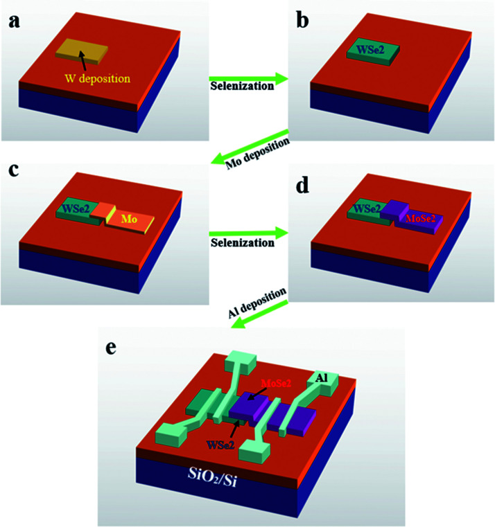
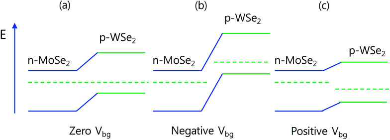
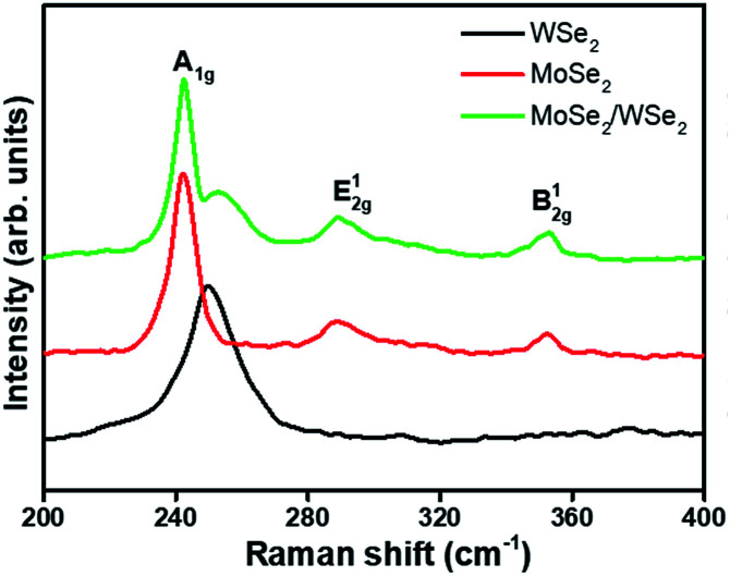
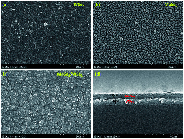
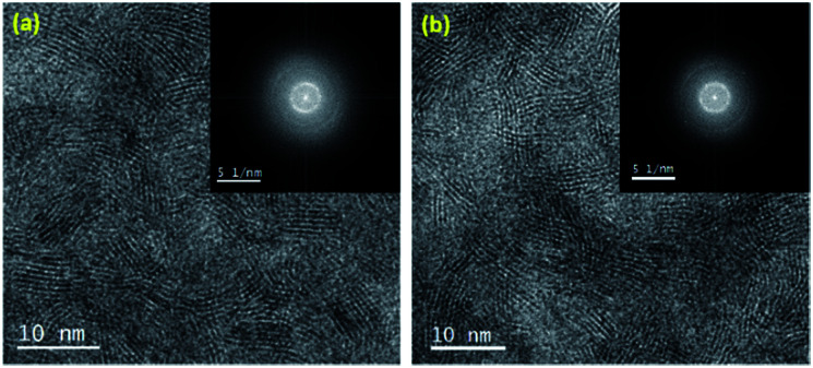
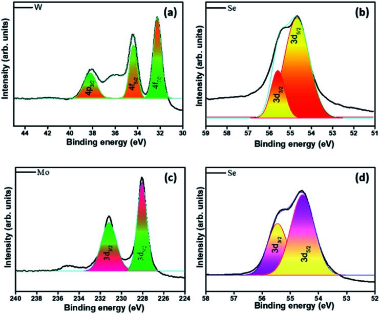
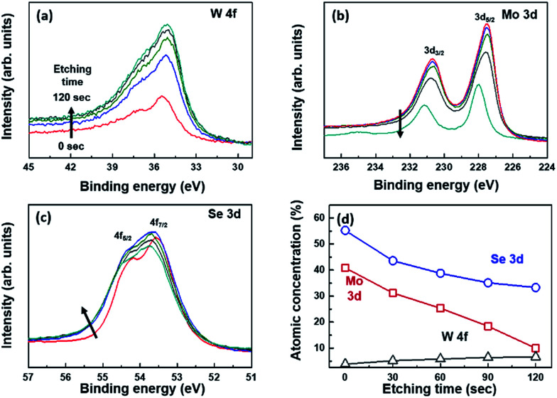
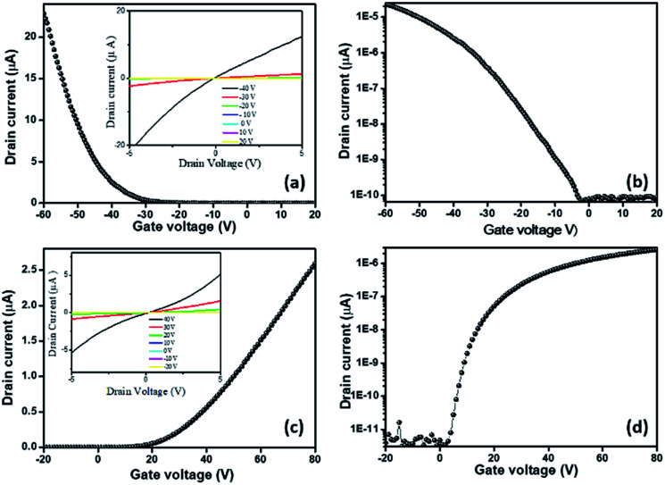
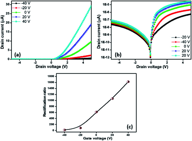
Here, we report the synthesis of a vertical MoSe/WSe p-n heterostructure using a sputtering-CVD method. Unlike the conventional CVD method, this method produced a continuous MoSe/WSe p-n heterostructure. WSe and MoSe back-gated field effect transistors (FETs) exhibited good gate modulation behavior, and high hole and electron mobilities of ∼2.2 and ∼15.1 cm V s, respectively. The fabricated vertical MoSe/WSe p-n diode showed rectifying - behavior with back-gate tunability. The rectification ratio of the diode was increased with increasing gate voltage, and was increased from ∼18 to ∼1600 as the gate bias increased from -40 V to +40 V. This is attributed to the fact that the barrier height between p-WSe and n-MoSe is modulated due to the back-gate bias. The rectification ratio is higher than the previously reported values for the TMDC p-n heterostructure grown by CVD.
在此,我们报道了一种采用溅射化学气相沉积(sputtering-CVD)方法合成垂直MoSe/WSe p-n异质结构的过程。与传统的化学气相沉积方法不同,该方法制备出了连续的MoSe/WSe p-n异质结构。WSe和MoSe背栅场效应晶体管(FET)表现出良好的栅极调制行为,空穴和电子迁移率分别高达约2.2 cm² V⁻¹ s⁻¹和约15.1 cm² V⁻¹ s⁻¹。所制备的垂直MoSe/WSe p-n二极管呈现出具有背栅可调性的整流行为。二极管的整流比随着栅极电压的增加而增大,当栅极偏压从-40 V增加到+40 V时,整流比从约18增大到约1600。这归因于背栅偏压调制了p-WSe和n-MoSe之间的势垒高度。该整流比高于之前报道的通过化学气相沉积生长的过渡金属二硫属化物p-n异质结构的值。