• 文献检索
  • 文档翻译
  • 深度研究
  • 学术资讯
  • Suppr Zotero 插件Zotero 插件
  • 邀请有礼
  • 套餐&价格
  • 历史记录
应用&插件
Suppr Zotero 插件Zotero 插件浏览器插件Mac 客户端Windows 客户端微信小程序
定价
高级版会员购买积分包购买API积分包
服务
文献检索文档翻译深度研究API 文档MCP 服务
关于我们
关于 Suppr公司介绍联系我们用户协议隐私条款
关注我们

Suppr 超能文献

核心技术专利:CN118964589B侵权必究
粤ICP备2023148730 号-1Suppr @ 2026

文献检索

告别复杂PubMed语法,用中文像聊天一样搜索,搜遍4000万医学文献。AI智能推荐,让科研检索更轻松。

立即免费搜索

文件翻译

保留排版,准确专业,支持PDF/Word/PPT等文件格式,支持 12+语言互译。

免费翻译文档

深度研究

AI帮你快速写综述,25分钟生成高质量综述,智能提取关键信息,辅助科研写作。

立即免费体验

作为一种用于外延微晶三维倒易空间映射的工具的拉东变换。

The Radon transform as a tool for 3D reciprocal-space mapping of epitaxial microcrystals.

作者信息

Meduňa Mojmír, Isa Fabio, Bressan Franco, von Känel Hans

机构信息

Department of Condensed Matter Physics, Masaryk University, Kotlářská 2, CZ-61137 Brno, Czech Republic.

Laboratory for Solid State Physics, ETH Zurich, Otto-Stern Weg 1, CH-8093 Zurich, Switzerland.

出版信息

J Appl Crystallogr. 2022 Jul 5;55(Pt 4):823-836. doi: 10.1107/S1600576722004885. eCollection 2022 Aug 1.

DOI:10.1107/S1600576722004885
PMID:35974728
原文链接:https://pmc.ncbi.nlm.nih.gov/articles/PMC9348889/
Abstract

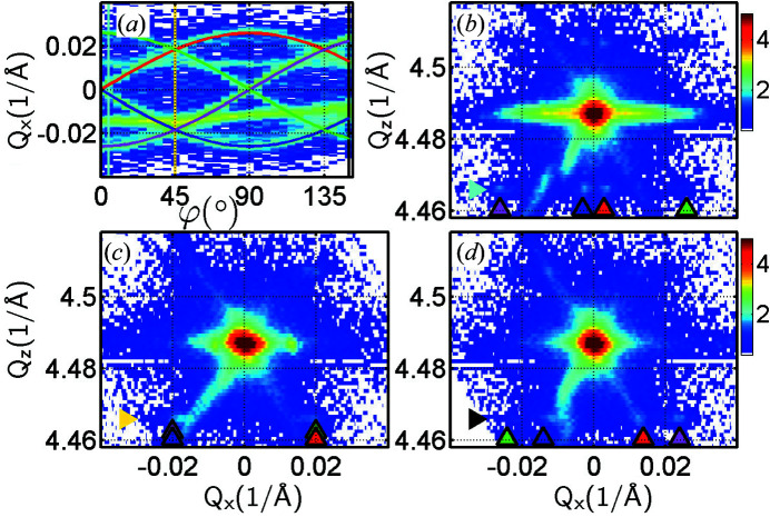
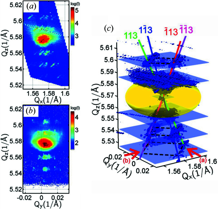
This work presents a new approach suitable for mapping reciprocal space in three dimensions with standard laboratory equipment and a typical X-ray diffraction setup. The method is based on symmetric and coplanar high-resolution X-ray diffraction, ideally realized using 2D X-ray pixel detectors. The processing of experimental data exploits the Radon transform commonly used in medical and materials science. It is shown that this technique can also be used for diffraction mapping in reciprocal space even if a highly collimated beam is not available. The application of the method is demonstrated for various types of epitaxial microcrystals on Si substrates. These comprise partially fused SiGe microcrystals that are tens of micrometres high, multiple-quantum-well structures grown on SiGe microcrystals and pyramid-shaped GaAs/Ge microcrystals on top of Si micropillars.

摘要

这项工作提出了一种新方法,适用于使用标准实验室设备和典型的X射线衍射装置在三维空间中映射倒易空间。该方法基于对称共面高分辨率X射线衍射,理想情况下使用二维X射线像素探测器来实现。实验数据的处理利用了医学和材料科学中常用的拉东变换。结果表明,即使没有高度准直的光束,该技术也可用于倒易空间中的衍射映射。该方法在硅衬底上的各种外延微晶上的应用得到了证明。这些包括几十微米高的部分熔融硅锗微晶、生长在硅锗微晶上的多量子阱结构以及硅微柱顶部的金字塔形砷化镓/锗微晶。

https://cdn.ncbi.nlm.nih.gov/pmc/blobs/2704/9348889/f7195e741d97/j-55-00823-fig12.jpg
https://cdn.ncbi.nlm.nih.gov/pmc/blobs/2704/9348889/7a8dae9dae0e/j-55-00823-fig1.jpg
https://cdn.ncbi.nlm.nih.gov/pmc/blobs/2704/9348889/39eba11da260/j-55-00823-fig2.jpg
https://cdn.ncbi.nlm.nih.gov/pmc/blobs/2704/9348889/583d77104721/j-55-00823-fig3.jpg
https://cdn.ncbi.nlm.nih.gov/pmc/blobs/2704/9348889/7a0bcf03bb4c/j-55-00823-fig4.jpg
https://cdn.ncbi.nlm.nih.gov/pmc/blobs/2704/9348889/50bb8fc1cb15/j-55-00823-fig5.jpg
https://cdn.ncbi.nlm.nih.gov/pmc/blobs/2704/9348889/c41c786e7fd7/j-55-00823-fig6.jpg
https://cdn.ncbi.nlm.nih.gov/pmc/blobs/2704/9348889/ad8eaed124d8/j-55-00823-fig7.jpg
https://cdn.ncbi.nlm.nih.gov/pmc/blobs/2704/9348889/d9d182c69adc/j-55-00823-fig8.jpg
https://cdn.ncbi.nlm.nih.gov/pmc/blobs/2704/9348889/ee19495a0056/j-55-00823-fig9.jpg
https://cdn.ncbi.nlm.nih.gov/pmc/blobs/2704/9348889/fa94e73f25c0/j-55-00823-fig10.jpg
https://cdn.ncbi.nlm.nih.gov/pmc/blobs/2704/9348889/4c044ca7cc98/j-55-00823-fig11.jpg
https://cdn.ncbi.nlm.nih.gov/pmc/blobs/2704/9348889/f7195e741d97/j-55-00823-fig12.jpg

相似文献

1
The Radon transform as a tool for 3D reciprocal-space mapping of epitaxial microcrystals.作为一种用于外延微晶三维倒易空间映射的工具的拉东变换。
J Appl Crystallogr. 2022 Jul 5;55(Pt 4):823-836. doi: 10.1107/S1600576722004885. eCollection 2022 Aug 1.
2
Characterization of SiGe thin films using a laboratory X-ray instrument.使用实验室X射线仪器对硅锗薄膜进行表征。
J Appl Crystallogr. 2013 Aug 1;46(Pt 4):898-902. doi: 10.1107/S0021889813010492. Epub 2013 Jun 7.
3
Defect free strain relaxation of microcrystals on mesoporous patterned silicon.介孔图案化硅上微晶的无缺陷应变弛豫
Nat Commun. 2022 Nov 4;13(1):6624. doi: 10.1038/s41467-022-34288-4.
4
Designing a standard for strain mapping: HR-EBSD analysis of SiGe thin film structures on Si.设计应变映射标准:硅上锗硅薄膜结构的高分辨率电子背散射衍射分析
Ultramicroscopy. 2015 Jan;148:94-104. doi: 10.1016/j.ultramic.2014.09.007. Epub 2014 Sep 30.
5
Epitaxial Growth of Ordered In-Plane Si and Ge Nanowires on Si (001).有序平面内硅和锗纳米线在硅(001)上的外延生长。
Nanomaterials (Basel). 2021 Mar 19;11(3):788. doi: 10.3390/nano11030788.
6
Heterogeneous integration of epitaxial Ge on Si using AlAs/GaAs buffer architecture: suitability for low-power fin field-effect transistors.采用AlAs/GaAs缓冲结构在硅上进行外延锗的异质集成:适用于低功耗鳍式场效应晶体管。
Sci Rep. 2014 Nov 7;4:6964. doi: 10.1038/srep06964.
7
Faceting of Si and Ge crystals grown on deeply patterned Si substrates in the kinetic regime: phase-field modelling and experiments.动力学条件下在深度图案化硅衬底上生长的硅和锗晶体的刻面化:相场建模与实验
Sci Rep. 2021 Sep 22;11(1):18825. doi: 10.1038/s41598-021-98285-1.
8
X-ray characterization of Ge dots epitaxially grown on nanostructured Si islands on silicon-on-insulator substrates.绝缘体上硅衬底上纳米结构硅岛外延生长的锗点的X射线表征
J Appl Crystallogr. 2013 Aug 1;46(Pt 4):868-873. doi: 10.1107/S0021889813003518. Epub 2013 Jun 7.
9
Structural Mapping of Functional Ge Layers Grown on Graded SiGe Buffers for sub-10 nm CMOS Applications Using Advanced X-ray Nanodiffraction.使用先进的 X 射线纳米衍射技术对用于亚 10nm CMOS 应用的渐变 SiGe 缓冲层上生长的功能 Ge 层进行结构映射。
ACS Appl Mater Interfaces. 2015 Dec 9;7(48):26696-700. doi: 10.1021/acsami.5b08645. Epub 2015 Nov 30.
10
Observation and understanding of anisotropic strain relaxation in selectively grown SiGe fin structures.选择性生长的 SiGe 鳍结构中各向异性应变弛豫的观察和理解。
Nanotechnology. 2017 Apr 7;28(14):145703. doi: 10.1088/1361-6528/aa5fbb. Epub 2017 Feb 10.

本文引用的文献

1
The characteristic radiation of copper Kα.铜Kα特征辐射
Acta Crystallogr A Found Adv. 2019 May 1;75(Pt 3):527-540. doi: 10.1107/S205327331900130X. Epub 2019 Apr 10.
2
Highly Mismatched, Dislocation-Free SiGe/Si Heterostructures.高度失配、无位错的 SiGe/Si 异质结构。
Adv Mater. 2016 Feb 3;28(5):884-8. doi: 10.1002/adma.201504029. Epub 2015 Dec 3.
3
Scanning X-ray strain microscopy of inhomogeneously strained Ge micro-bridges.非均匀应变锗微桥的扫描 X 射线应变显微镜。
J Synchrotron Radiat. 2014 Jan;21(Pt 1):111-8. doi: 10.1107/S1600577513025459. Epub 2013 Nov 2.
4
Perfect crystals grown from imperfect interfaces.从非完美界面生长出的完美晶体。
Sci Rep. 2013;3:2276. doi: 10.1038/srep02276.
5
Scaling hetero-epitaxy from layers to three-dimensional crystals.从层状到三维晶体的异质外延缩放。
Science. 2012 Mar 16;335(6074):1330-4. doi: 10.1126/science.1217666.
6
On the Determination of Functions from Their Integral Values along Certain Manifolds.关于从函数在某些流形上的积分值确定函数
IEEE Trans Med Imaging. 1986;5(4):170-6. doi: 10.1109/TMI.1986.4307775.
7
Nonspecular x-ray reflection from rough multilayers.来自粗糙多层膜的非镜面X射线反射。
Phys Rev B Condens Matter. 1994 Apr 15;49(15):10668-10676. doi: 10.1103/physrevb.49.10668.
8
X-ray reflection from rough layered systems.粗糙层状体系的X射线反射
Phys Rev B Condens Matter. 1993 Jun 15;47(23):15896-15903. doi: 10.1103/physrevb.47.15896.