Seewald Lukas Matthias, Sattelkow Jürgen, Brugger-Hatzl Michele, Kothleitner Gerald, Frerichs Hajo, Schwalb Christian, Hummel Stefan, Plank Harald
Christian Doppler Laboratory for Direct-Write Fabrication of 3D Nano-Probes, Graz University of Technology, 8010 Graz, Austria.
Institute of Electron Microscopy and Nanoanalysis, Graz University of Technology, 8010 Graz, Austria.
Nanomaterials (Basel). 2022 Dec 17;12(24):4477. doi: 10.3390/nano12244477.
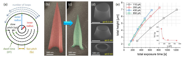
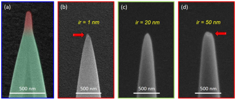
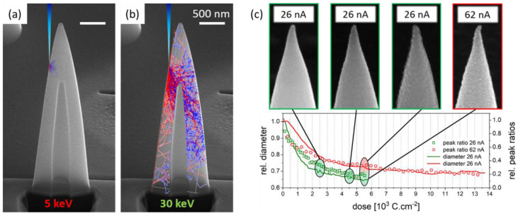
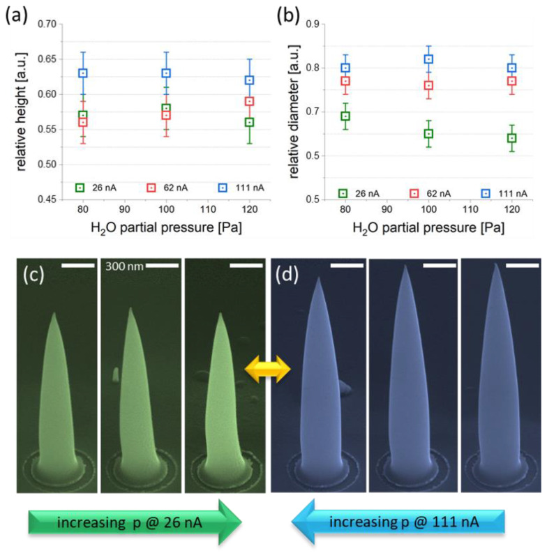
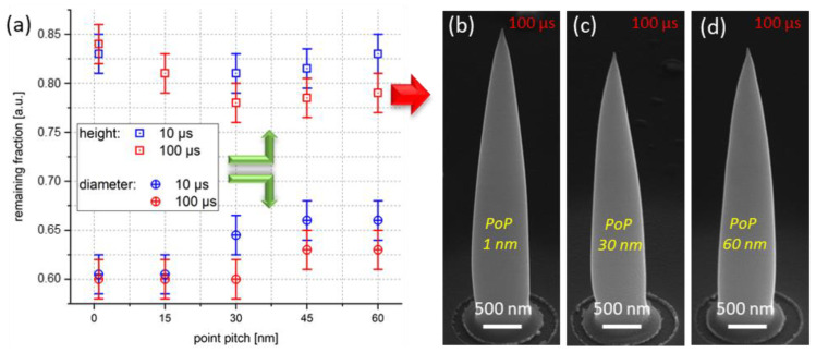
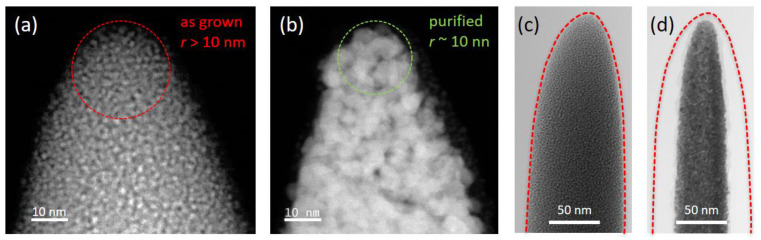
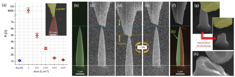
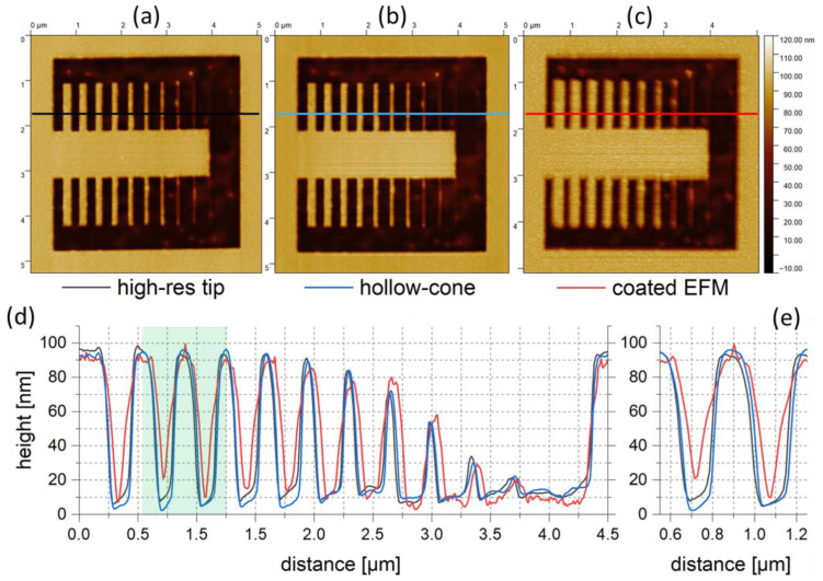
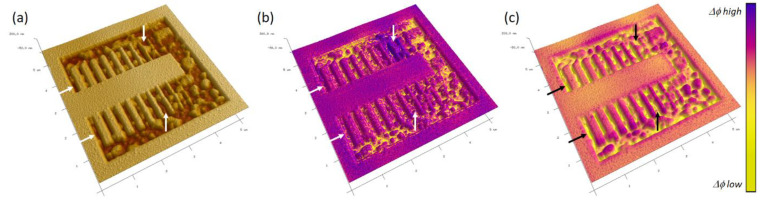
3D nanoprinting via focused electron beam induced deposition (FEBID) is applied for fabrication of all-metal nanoprobes for atomic force microscopy (AFM)-based electrical operation modes. The 3D tip concept is based on a hollow-cone (HC) design, with all-metal material properties and apex radii in the sub-10 nm regime to allow for high-resolution imaging during morphological imaging, conductive AFM (CAFM) and electrostatic force microscopy (EFM). The study starts with design aspects to motivate the proposed HC architecture, followed by detailed fabrication characterization to identify and optimize FEBID process parameters. To arrive at desired material properties, e-beam assisted purification in low-pressure water atmospheres was applied at room temperature, which enabled the removal of carbon impurities from as-deposited structures. The microstructure of final HCs was analyzed via scanning transmission electron microscopy-high-angle annular dark field (STEM-HAADF), whereas electrical and mechanical properties were investigated in situ using micromanipulators. Finally, AFM/EFM/CAFM measurements were performed in comparison to non-functional, high-resolution tips and commercially available electric probes. In essence, we demonstrate that the proposed all-metal HCs provide the resolution capabilities of the former, with the electric conductivity of the latter onboard, combining both assets in one design.
通过聚焦电子束诱导沉积(FEBID)进行的3D纳米打印被应用于制造用于基于原子力显微镜(AFM)的电操作模式的全金属纳米探针。3D尖端概念基于空心锥(HC)设计,具有全金属材料特性且顶点半径在亚10纳米范围内,以便在形态成像、导电原子力显微镜(CAFM)和静电力显微镜(EFM)过程中实现高分辨率成像。该研究首先从设计方面入手以推动所提出的HC架构,随后进行详细的制造表征以识别和优化FEBID工艺参数。为了获得所需的材料特性,在室温下于低压水气氛中应用电子束辅助纯化,这能够从沉积后的结构中去除碳杂质。通过扫描透射电子显微镜-高角度环形暗场(STEM-HAADF)分析最终HC的微观结构,而使用微操纵器原位研究其电学和力学性能。最后,与非功能性高分辨率尖端和市售电探针相比进行了AFM/EFM/CAFM测量。本质上,我们证明所提出的全金属HC兼具前者的分辨率能力以及后者的导电性,在一种设计中融合了这两种特性。