Plank Harald, Winkler Robert, Schwalb Christian H, Hütner Johanna, Fowlkes Jason D, Rack Philip D, Utke Ivo, Huth Michael
Christian Doppler Laboratory for Direct-Write Fabrication of 3D Nano-Probes (DEFINE), Institute of Electron Microscopy and Nanoanalysis, Graz University of Technology, 8010 Graz, Austria.
Institute of Electron Microscopy and Nanoanalysis, Graz University of Technology, 8010 Graz, Austria.
Micromachines (Basel). 2019 Dec 30;11(1):48. doi: 10.3390/mi11010048.
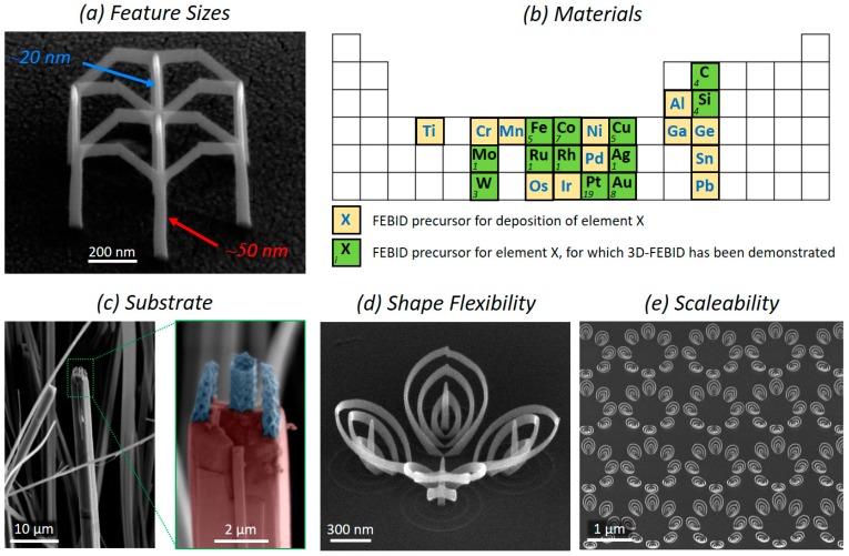
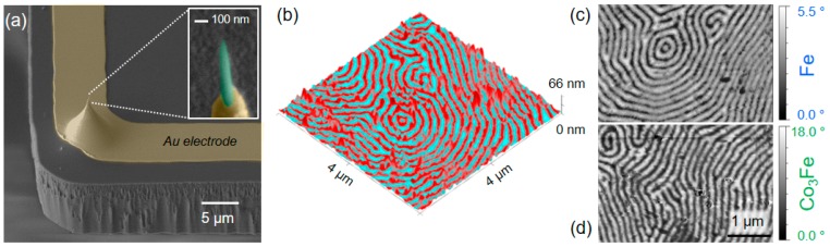
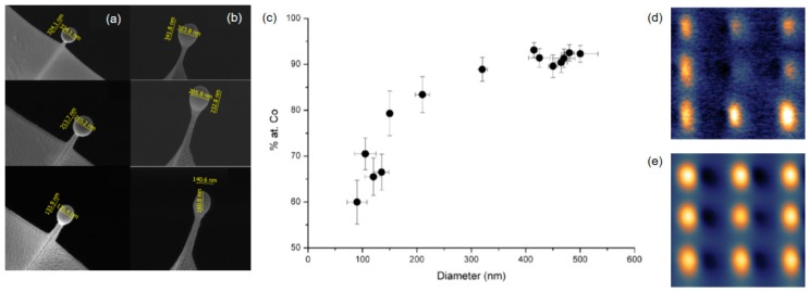
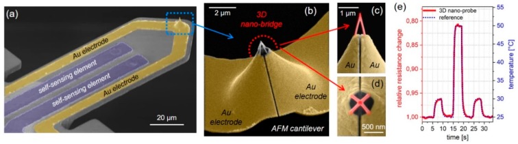
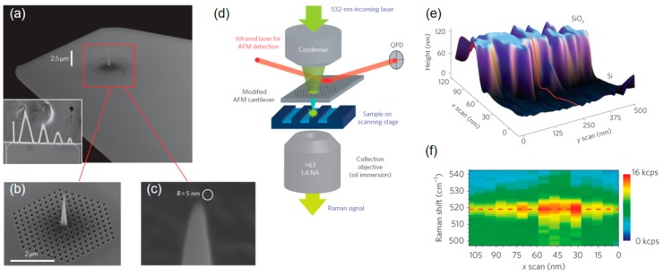
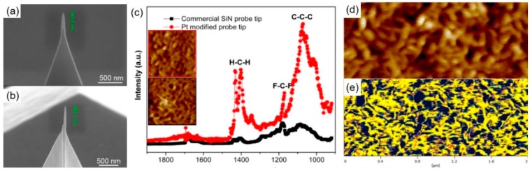
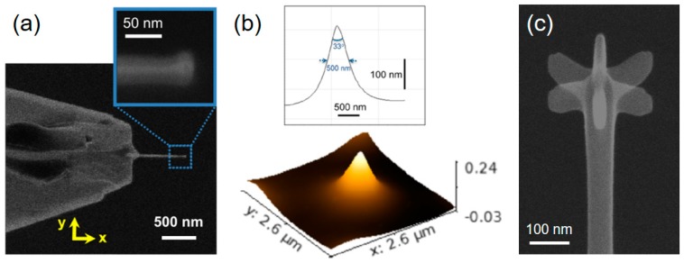
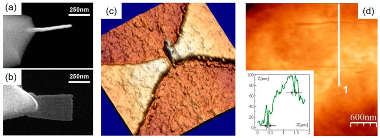
Scanning probe microscopy (SPM) has become an essential surface characterization technique in research and development. By concept, SPM performance crucially depends on the quality of the nano-probe element, in particular, the apex radius. Now, with the development of advanced SPM modes beyond morphology mapping, new challenges have emerged regarding the design, morphology, function, and reliability of nano-probes. To tackle these challenges, versatile fabrication methods for precise nano-fabrication are needed. Aside from well-established technologies for SPM nano-probe fabrication, focused electron beam-induced deposition (FEBID) has become increasingly relevant in recent years, with the demonstration of controlled 3D nanoscale deposition and tailored deposit chemistry. Moreover, FEBID is compatible with practically any given surface morphology. In this review article, we introduce the technology, with a focus on the most relevant demands (shapes, feature size, materials and functionalities, substrate demands, and scalability), discuss the opportunities and challenges, and rationalize how those can be useful for advanced SPM applications. As will be shown, FEBID is an ideal tool for fabrication / modification and rapid prototyping of SPM-tipswith the potential to scale up industrially relevant manufacturing.
扫描探针显微镜(SPM)已成为研发中一种重要的表面表征技术。从概念上讲,SPM的性能关键取决于纳米探针元件的质量,尤其是针尖半径。如今,随着超越形貌映射的先进SPM模式的发展,纳米探针的设计、形貌、功能和可靠性方面出现了新的挑战。为应对这些挑战,需要用于精确纳米制造的通用制造方法。除了成熟的SPM纳米探针制造技术外,聚焦电子束诱导沉积(FEBID)近年来变得越来越重要,它展示了可控的三维纳米级沉积和定制的沉积化学性质。此外,FEBID与几乎任何给定的表面形貌都兼容。在这篇综述文章中,我们介绍这项技术,重点关注最相关的要求(形状、特征尺寸、材料和功能、衬底要求以及可扩展性),讨论机遇和挑战,并阐述其如何能用于先进的SPM应用。如将展示的那样,FEBID是用于SPM针尖制造/修饰和快速原型制作的理想工具,具有扩大工业相关制造规模的潜力。