Nawwar Mohamed A, Abo Ghazala Magdy S, Sharaf El-Deen Lobna M, Anis Badawi, El-Shaer Abdelhamid, Elseman Ahmed Mourtada, Rashad Mohamed M, Kashyout Abd El-Hady B
Physics Department, Faculty of Science, Menoufia University Shebin El-Koom Menoufia 32511 Egypt
Spectroscopy Department, Physics Research Institute, National Research Centre 33 El Bohouth St., Dokki 12622 Giza Egypt.
RSC Adv. 2023 Mar 20;13(14):9154-9167. doi: 10.1039/d3ra00805c.
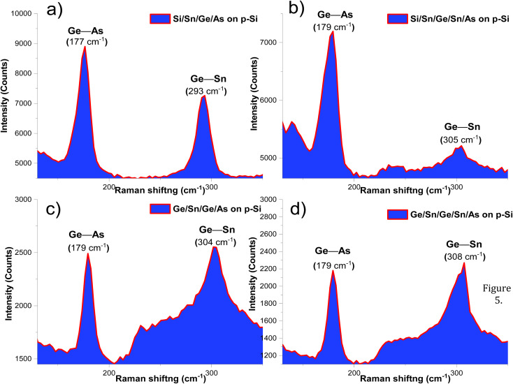
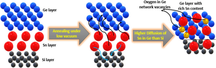
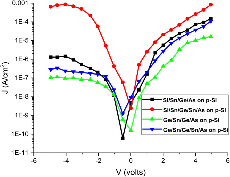
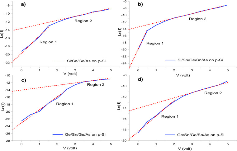
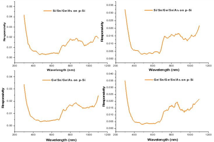
GeSn compounds have made many interesting contributions in photodetectors (PDs) over the last ten years, as they have a detection limit in the NIR and mid-IR region. Sn incorporation in Ge alters the cut off wavelength. In the present article, p-i-n structures based on GeSn junctions were fabricated to serve as PDs. Arsine (As) is incorporated to develop n-GeSn compounds a metal induced crystallization (MIC) process followed by i-GeSn on p-Si wafers. The impact of As and Sn doping on the strain characteristics of GeSn has been studied with high resolution transmission electron microscopy (HRTEM), X-ray diffraction and Raman spectroscopy analyses. The direct transitions and tuning of their band energies have been investigated using diffuse reflectance UV-vis spectroscopy and photoluminescence (PL). The barrier height and spectral responsivity have been controlled with incorporation of As. Variation of As incorporation into GeSn Compounds shifted the Raman peak and hence affected the strain in the Ge network. UV-vis spectroscopy showed that the direct transition energies are lowered as the Ge-As bonding increases as illustrated in Raman spectroscopy investigations. PL and UV-vis spectroscopy of annealed heterostructures at 500 °C showed that there are many transition peaks from the UV to the NIR region as result of oxygen vacancies in the Ge network. The calculated diode parameters showed that As incorporation leads to an increase of the height barrier and thus dark current. Spectral response measurements show that the prepared heterojunctions have spectral responses in near UV and NIR regions that gives them opportunities in UV and NIR photodetection-applications.
在过去十年中,锗锡化合物在光电探测器(PD)领域做出了许多有趣的贡献,因为它们在近红外和中红外区域具有检测极限。在锗中掺入锡会改变截止波长。在本文中,制备了基于锗锡结的p-i-n结构用作光电探测器。通过在p型硅晶圆上采用金属诱导结晶(MIC)工艺,然后生长i-GeSn,掺入砷(As)来制备n-GeSn化合物。利用高分辨率透射电子显微镜(HRTEM)、X射线衍射和拉曼光谱分析研究了砷和锡掺杂对锗锡应变特性的影响。使用漫反射紫外可见光谱和光致发光(PL)研究了它们的直接跃迁和能带能量的调谐。通过掺入砷来控制势垒高度和光谱响应率。砷掺入锗锡化合物中的变化使拉曼峰发生位移,从而影响锗网络中的应变。紫外可见光谱表明,正如拉曼光谱研究所表明的那样,随着Ge-As键合增加,直接跃迁能量降低。对在500°C退火的异质结构进行的PL和紫外可见光谱表明,由于锗网络中的氧空位,从紫外到近红外区域有许多跃迁峰。计算得到的二极管参数表明,掺入砷会导致势垒高度增加,从而使暗电流增加。光谱响应测量表明,制备的异质结在近紫外和近红外区域具有光谱响应,这为它们在紫外和近红外光探测应用中提供了机会。