Zendrini Michele, Dubrovskii Vladimir, Rudra Alok, Dede Didem, Fontcuberta I Morral Anna, Piazza Valerio
Laboratory of Semiconductor Materials, Institute of Materials, Ecole Polytechnique Fédérale de Lausanne (EPFL), Lausanne CH-1015, Switzerland.
Faculty of Physics, St. Petersburg State University, Universitetskaya Emb. 13B, St. Petersburg 199034, Russia.
ACS Appl Nano Mater. 2024 Aug 13;7(16):19065-19074. doi: 10.1021/acsanm.4c02765. eCollection 2024 Aug 23.
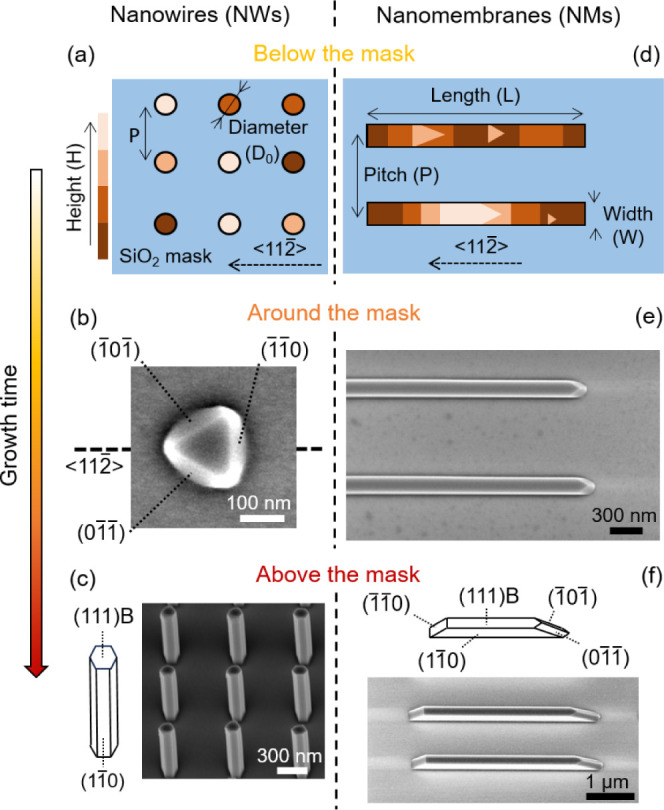
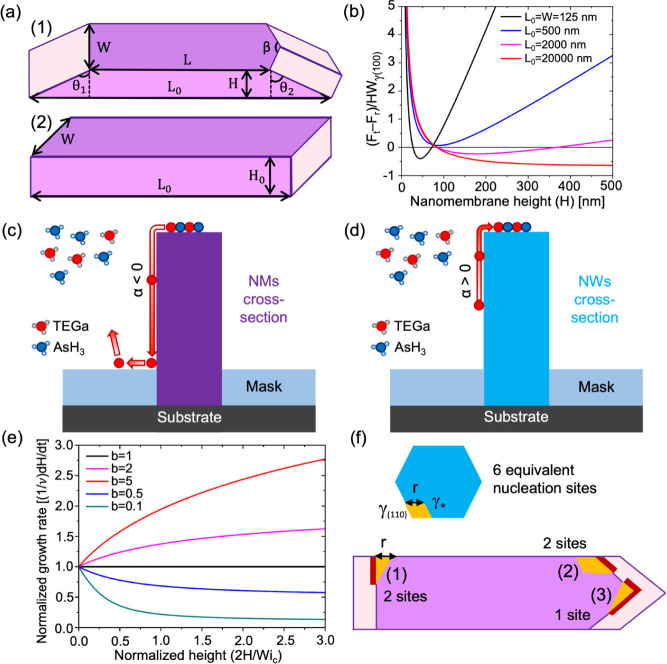
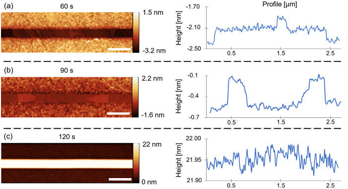
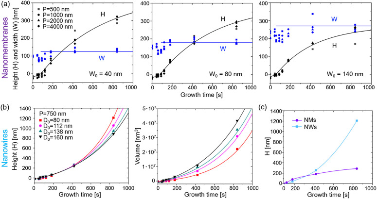
The growth kinetics of vertical III-V nanowires (NWs) were clarified long ago. The increasing aspect ratio of NWs results in an increase in the surface area, which, in turn, enhances the material collection. The group III adatom diffusion from the NW sidewalls to the top sustains a superlinear growth regime. In this work, we report on the growth of different GaAs nanostructures by selective area MOVPE on GaAs (111)B substrates. We show that the opening dimensions and geometry qualitatively alter the morphology and height evolution of the structures. We compare the time evolution of vertical GaAs NWs stemming from circular holes and horizontal GaAs nanomembranes (NMs) growing from one-dimensional (1D) rectangular slits on the same substrate. While NW heights grow exponentially with time, NMs surprisingly exhibit sublinear kinetics. The absence of visible atomic steps on the top facets of both NWs and NMs suggests layer-by-layer growth in the mononuclear mode. We interpret these observations within a self-consistent growth model, which links the diffusion flux of Ga adatoms to the position- and shape-dependent nucleation rate on top of NWs and NMs. Specifically, the island nucleation rate is lower on top of the NMs than that on the NWs, resulting in the total diffusion flux being directed from the top facet to the sidewalls. This gives a sublinear height evolution for the NMs. These results open innovative perspectives for shape engineering of III-V nanostructures and new avenues for the design of optoelectronics and photonic devices.
垂直III-V族纳米线(NWs)的生长动力学早在很久以前就已阐明。NWs纵横比的增加导致表面积增大,进而提高了材料收集效率。III族吸附原子从NWs侧壁扩散到顶部维持了超线性生长模式。在这项工作中,我们报道了通过在GaAs(111)B衬底上进行选择性区域金属有机气相外延(MOVPE)生长不同的GaAs纳米结构。我们表明,开口尺寸和几何形状定性地改变了结构的形态和高度演变。我们比较了源自圆形孔的垂直GaAs NWs和在同一衬底上从一维(1D)矩形狭缝生长的水平GaAs纳米膜(NMs)的时间演变。虽然NWs的高度随时间呈指数增长,但NMs令人惊讶地表现出亚线性动力学。NWs和NMs顶部小平面上均没有可见的原子台阶,这表明是单核模式下的逐层生长。我们在一个自洽的生长模型中解释这些观察结果,该模型将Ga吸附原子的扩散通量与NWs和NMs顶部位置和形状相关的成核速率联系起来。具体而言,NMs顶部的岛状成核速率低于NWs顶部的成核速率,导致总扩散通量从顶部小平面指向侧壁。这使得NMs的高度演变呈亚线性。这些结果为III-V族纳米结构的形状工程开辟了创新视角,并为光电子和光子器件的设计提供了新途径。