Zhang Xutao, Zhang Fanlu, Yi Ruixuan, Wang Naiyin, Su Zhicheng, Zhang Mingwen, Zhao Bijun, Li Ziyuan, Qu Jiangtao, M Cairney Julie, Lu Yuerui, Zhao Jianlin, Gan Xuetao, Tan Hark Hoe, Jagadish Chennupati, Fu Lan
Frontiers Science Center for Flexible Electronics, Xi'an Institute of Flexible Electronics (IFE) and Xi'an Institute of Biomedical Materials & Engineering, Northwestern Polytechnical University, 127 West Youyi Road, 710072, Xi'an, China.
Department of Electronic Materials Engineering, Research School of Physics, The Australian National University, Canberra, ACT 2600, Australia.
Light Sci Appl. 2024 Sep 4;13(1):230. doi: 10.1038/s41377-024-01570-7.
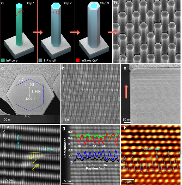
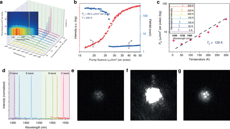
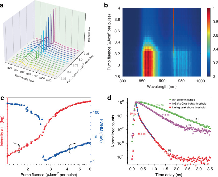
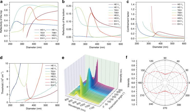
Highly integrated optoelectronic and photonic systems underpin the development of next-generation advanced optical and quantum communication technologies, which require compact, multiwavelength laser sources at the telecom band. Here, we report on-substrate vertical emitting lasing from ordered InGaAs/InP multi-quantum well core-shell nanowire array epitaxially grown on InP substrate by selective area epitaxy. To reduce optical loss and tailor the cavity mode, a new nanowire facet engineering approach has been developed to achieve controlled quantum well nanowire dimensions with uniform morphology and high crystal quality. Owing to the strong quantum confinement effect of InGaAs quantum wells and the successful formation of a vertical Fabry-Pérot cavity between the top nanowire facet and bottom nanowire/SiO mask interface, stimulated emissions of the EH mode from single vertical nanowires from an on-substrate nanowire array have been demonstrated with a lasing threshold of ~28.2 μJ cm per pulse and a high characteristic temperature of ~128 K. By fine-tuning the In composition of the quantum wells, room temperature, single-mode lasing is achieved in the vertical direction across a broad near-infrared spectral range, spanning from 940 nm to the telecommunication O and C bands. Our research indicates that through a carefully designed facet engineering strategy, highly ordered, uniform nanowire arrays with precise dimension control can be achieved to simultaneously deliver thousands of nanolasers with multiple wavelengths on the same substrate, paving a promising and scalable pathway towards future advanced optoelectronic and photonic systems.
高度集成的光电和光子系统是下一代先进光学和量子通信技术发展的基础,这些技术需要紧凑的电信波段多波长激光源。在此,我们报道了通过选择性区域外延在磷化铟(InP)衬底上外延生长的有序铟镓砷(InGaAs)/InP多量子阱核壳纳米线阵列的衬底上垂直发射激光。为了降低光损耗并调整腔模,已开发出一种新的纳米线刻面工程方法,以实现具有均匀形态和高晶体质量的可控量子阱纳米线尺寸。由于InGaAs量子阱的强量子限制效应以及在顶部纳米线刻面与底部纳米线/二氧化硅(SiO)掩膜界面之间成功形成垂直法布里-珀罗腔,已证明来自衬底上纳米线阵列中单个垂直纳米线的EH模式受激发射,其激光阈值约为每脉冲28.2微焦每平方厘米,特征温度约为128 K。通过微调量子阱的铟成分,在从940 nm到电信O和C波段的宽近红外光谱范围内,在垂直方向上实现了室温单模激光发射。我们的研究表明,通过精心设计的刻面工程策略,可以实现具有精确尺寸控制的高度有序、均匀的纳米线阵列,从而在同一衬底上同时提供数千个多波长纳米激光器,为未来先进的光电和光子系统铺平了一条有前景且可扩展的道路。