Tian Ruijuan, Zhang Yong, Ji Yingke, Li Chen, Wu Xianghu, Wang Jianguo, Jia Shuaiwei, Liu Liang, Zhang Mingwen, Zhang Yu, Zhang Qiao, Xie Zhuang, Luo Zhengdong, Gao Duorui, Liu Yan, Zhao Jianlin, Sun Zhipei, Gan Xuetao
Key Laboratory of Light Field Manipulation and Information Acquisition, and Shaanxi Key Laboratory of Optical Information Technology, School of Physical Science and Technology, Northwestern Polytechnical University, Xi'an, China.
Department of Electronics and Nanoengineering, Aalto University, Espoo, Finland.
Light Sci Appl. 2025 Jul 7;14(1):238. doi: 10.1038/s41377-025-01832-y.
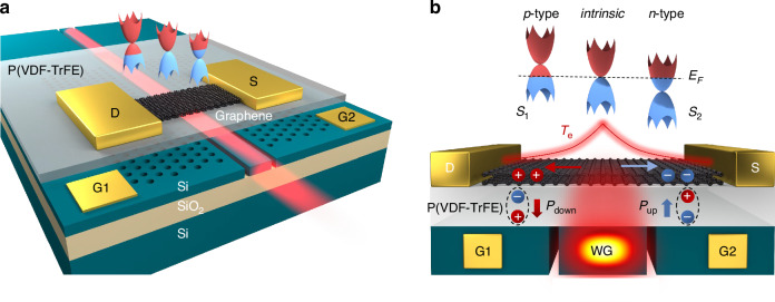
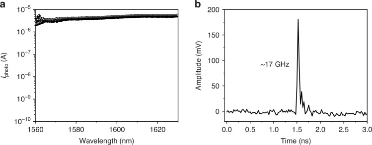
Graphene's unique photothermoelectric (PTE) effect, combined with its compatibility for on-chip fabrication, promises its development in chip-integrated photodetectors with ultralow dark-current and ultrafast speed. Previous designs of on-chip graphene photodetectors required external electrical biases or gate voltages to separate photocarriers, leading to increased power consumption and complex circuitry. Here, we demonstrate a nonvolatile graphene p-i-n homojunction constructed on a silicon photonic crystal waveguide, which facilitates PTE-based photodetection without the need for electrical bias or gate voltages. By designing an air-slotted photonic crystal waveguide as two individual silicon back gates and employing ferroelectric dielectrics with remnant polarization fields, the nonvolatile p-i-n homojunction with a clear gradient of Seebeck coefficient is electrically configured. Hot carriers in the graphene channel generated from the absorption of waveguide evanescent field are separated by the nonvolatile p-i-n homojunction effectively to yield considerable photocurrents. With zero-bias and zero-gate voltage, the nonvolatile graphene p-i-n homojunction photodetector integrated on the optical waveguide exhibits high and flat responsivity of 193 mA W over the broadband wavelength range of 1560-1630 nm and an ultrafast dynamics bandwidth of 17 GHz measured in the limits of our instruments. With the high-performance on-chip photodetection, the nonvolatile graphene homojunction directly constructed on silicon photonic circuits promises the extended on-chip functions of the optoelectronic synapse, in-memory sensing and computing, and neuromorphic computing.
石墨烯独特的光热电(PTE)效应,结合其与片上制造的兼容性,有望推动其在具有超低暗电流和超快速度的片上集成光电探测器中的发展。以往的片上石墨烯光电探测器设计需要外部电偏置或栅极电压来分离光载流子,导致功耗增加和电路复杂。在此,我们展示了一种构建在硅光子晶体波导上的非易失性石墨烯p-i-n同质结,它无需电偏置或栅极电压即可实现基于PTE的光电探测。通过将空气隙光子晶体波导设计为两个独立的硅背栅,并采用具有剩余极化场的铁电介质,实现了具有清晰塞贝克系数梯度的非易失性p-i-n同质结的电配置。由波导倏逝场吸收产生的石墨烯通道中的热载流子被非易失性p-i-n同质结有效分离,从而产生可观的光电流。在零偏置和零栅极电压下,集成在光波导上的非易失性石墨烯p-i-n同质结光电探测器在1560 - 1630 nm的宽带波长范围内表现出193 mA W的高且平坦的响应度,以及在我们仪器测量极限下为17 GHz的超快动力学带宽。凭借这种高性能的片上光电探测,直接构建在硅光子电路上的非易失性石墨烯同质结有望实现光电突触、内存中传感与计算以及神经形态计算等扩展的片上功能。