• 文献检索
  • 文档翻译
  • 深度研究
  • 学术资讯
  • Suppr Zotero 插件Zotero 插件
  • 邀请有礼
  • 套餐&价格
  • 历史记录
应用&插件
Suppr Zotero 插件Zotero 插件浏览器插件Mac 客户端Windows 客户端微信小程序
定价
高级版会员购买积分包购买API积分包
服务
文献检索文档翻译深度研究API 文档MCP 服务
关于我们
关于 Suppr公司介绍联系我们用户协议隐私条款
关注我们

Suppr 超能文献

核心技术专利:CN118964589B侵权必究
粤ICP备2023148730 号-1Suppr @ 2026

文献检索

告别复杂PubMed语法,用中文像聊天一样搜索,搜遍4000万医学文献。AI智能推荐,让科研检索更轻松。

立即免费搜索

文件翻译

保留排版,准确专业,支持PDF/Word/PPT等文件格式,支持 12+语言互译。

免费翻译文档

深度研究

AI帮你快速写综述,25分钟生成高质量综述,智能提取关键信息,辅助科研写作。

立即免费体验

使用哪种光电二极管:CMOS兼容结构的比较

Which Photodiode to Use: A Comparison of CMOS-Compatible Structures.

作者信息

Murari Kartikeya, Etienne-Cummings Ralph, Thakor Nitish, Cauwenberghs Gert

机构信息

Department of Biomedical Engineering, Johns Hopkins University School of Medicine, Baltimore, MD 21205 USA.

出版信息

IEEE Sens J. 2009 Jul 1;9(7):752-760. doi: 10.1109/JSEN.2009.2021805.

DOI:10.1109/JSEN.2009.2021805
PMID:20454596
原文链接:https://pmc.ncbi.nlm.nih.gov/articles/PMC2863350/
Abstract

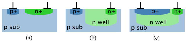
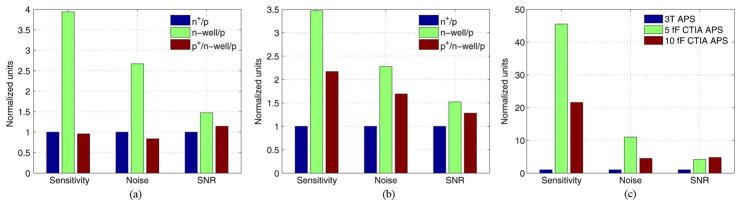
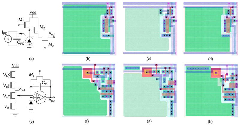
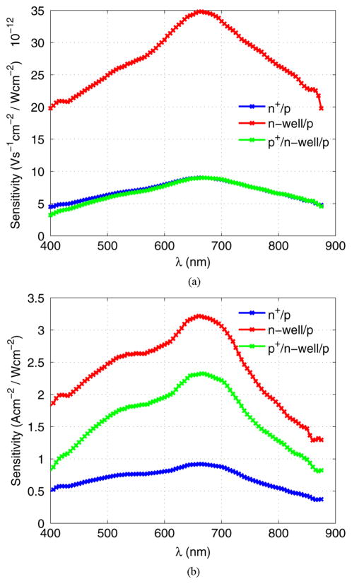
While great advances have been made in optimizing fabrication process technologies for solid state image sensors, the need remains to be able to fabricate high quality photosensors in standard CMOS processes. The quality metrics depend on both the pixel architecture and the photosensitive structure. This paper presents a comparison of three photodiode structures in terms of spectral sensitivity, noise and dark current. The three structures are n(+)/p-sub, n-well/p-sub and p(+)/n-well/p-sub. All structures were fabricated in a 0.5 mum 3-metal, 2-poly, n-well process and shared the same pixel and readout architectures. Two pixel structures were fabricated-the standard three transistor active pixel sensor, where the output depends on the photodiode capacitance, and one incorporating an in-pixel capacitive transimpedance amplifier where the output is dependent only on a designed feedback capacitor. The n-well/p-sub diode performed best in terms of sensitivity (an improvement of 3.5 x and 1.6 x over the n(+)/p-sub and p(+)/n-well/p-sub diodes, respectively) and signal-to-noise ratio (1.5 x and 1.2 x improvement over the n(+)/p-sub and p(+)/n-well/p-sub diodes, respectively) while the p(+)/n-well/p-sub diode had the minimum (33% compared to other two structures) dark current for a given sensitivity.

摘要

虽然在优化固态图像传感器的制造工艺技术方面已经取得了巨大进展,但仍然需要能够在标准CMOS工艺中制造高质量的光电传感器。质量指标取决于像素架构和光敏结构。本文从光谱灵敏度、噪声和暗电流方面对三种光电二极管结构进行了比较。这三种结构分别是n(+)/p-衬底、n阱/p-衬底和p(+)/n阱/p-衬底。所有结构均采用0.5微米3金属、2多晶硅、n阱工艺制造,并共享相同的像素和读出架构。制造了两种像素结构——标准的三晶体管有源像素传感器,其输出取决于光电二极管电容;另一种包含像素内电容跨阻放大器,其输出仅取决于设计的反馈电容。n阱/p-衬底二极管在灵敏度(分别比n(+)/p-衬底和p(+)/n阱/p-衬底二极管提高3.5倍和1.6倍)和信噪比(分别比n(+)/p-衬底和p(+)/n阱/p-衬底二极管提高1.5倍和1.2倍)方面表现最佳,而在给定灵敏度下,p(+)/n阱/p-衬底二极管的暗电流最小(与其他两种结构相比为33%)。

https://cdn.ncbi.nlm.nih.gov/pmc/blobs/9741/2863350/26a2f817bc75/nihms175399f6.jpg
https://cdn.ncbi.nlm.nih.gov/pmc/blobs/9741/2863350/860729646adf/nihms175399f1.jpg
https://cdn.ncbi.nlm.nih.gov/pmc/blobs/9741/2863350/5a4fde8139fd/nihms175399f2.jpg
https://cdn.ncbi.nlm.nih.gov/pmc/blobs/9741/2863350/2653e9decf98/nihms175399f3.jpg
https://cdn.ncbi.nlm.nih.gov/pmc/blobs/9741/2863350/9a47830c2fe0/nihms175399f4.jpg
https://cdn.ncbi.nlm.nih.gov/pmc/blobs/9741/2863350/a8baffaa033e/nihms175399f5.jpg
https://cdn.ncbi.nlm.nih.gov/pmc/blobs/9741/2863350/26a2f817bc75/nihms175399f6.jpg

相似文献

1
Which Photodiode to Use: A Comparison of CMOS-Compatible Structures.使用哪种光电二极管:CMOS兼容结构的比较
IEEE Sens J. 2009 Jul 1;9(7):752-760. doi: 10.1109/JSEN.2009.2021805.
2
The Effect of Pixel Design and Operation Conditions on Linear Output Range of 4T CMOS Image Sensors.像素设计和操作条件对4T CMOS图像传感器线性输出范围的影响
Sensors (Basel). 2024 Mar 13;24(6):1841. doi: 10.3390/s24061841.
3
A CMOS In-Pixel CTIA High Sensitivity Fluorescence Imager.一种基于互补金属氧化物半导体(CMOS)的像素内电流积分型放大器(CTIA)高灵敏度荧光成像仪。
IEEE Trans Biomed Circuits Syst. 2011 Oct;5(5):449-458. doi: 10.1109/tbcas.2011.2114660. Epub 2011 Mar 24.
4
A 75-ps Gated CMOS Image Sensor with Low Parasitic Light Sensitivity.一款具有低寄生光灵敏度的75皮秒门控CMOS图像传感器。
Sensors (Basel). 2016 Jun 29;16(7):999. doi: 10.3390/s16070999.
5
A CMOS Optoelectronic Receiver IC with an On-Chip Avalanche Photodiode for Home-Monitoring LiDAR Sensors.一种用于家庭监测激光雷达传感器的带有片上雪崩光电二极管的CMOS光电接收器集成电路。
Sensors (Basel). 2021 Jun 25;21(13):4364. doi: 10.3390/s21134364.
6
A High Full Well Capacity CMOS Image Sensor for Space Applications.用于空间应用的高满阱容量 CMOS 图像传感器。
Sensors (Basel). 2019 Mar 28;19(7):1505. doi: 10.3390/s19071505.
7
A Low-Noise CMOS Transimpedance-Limiting Amplifier for Dynamic Range Extension.一种用于扩展动态范围的低噪声CMOS跨阻限幅放大器。
Micromachines (Basel). 2025 Jan 28;16(2):153. doi: 10.3390/mi16020153.
8
Automotive 2.1 μm Full-Depth Deep Trench Isolation CMOS Image Sensor with a 120 dB Single-Exposure Dynamic Range.具有120dB单曝光动态范围的汽车级2.1μm全深度深沟槽隔离CMOS图像传感器。
Sensors (Basel). 2023 Nov 13;23(22):9150. doi: 10.3390/s23229150.
9
An Over 90 dB Intra-Scene Single-Exposure Dynamic Range CMOS Image Sensor Using a 3.0 μm Triple-Gain Pixel Fabricated in a Standard BSI Process.一种采用标准背照式工艺制造的3.0μm三增益像素的90dB以上场景内单曝光动态范围CMOS图像传感器。
Sensors (Basel). 2018 Jan 12;18(1):203. doi: 10.3390/s18010203.
10
A Tunable-Gain Transimpedance Amplifier for CMOS-MEMS Resonators Characterization.一种用于CMOS-MEMS谐振器特性表征的可调增益跨阻放大器。
Micromachines (Basel). 2021 Jan 15;12(1):82. doi: 10.3390/mi12010082.

引用本文的文献

1
Integrated High-Temporal-Resolution and High-Density Subretinal Prosthesis Using a Correlated Double-Sampling Technique.采用相关双采样技术的集成高时间分辨率和高密度视网膜下假体。
Sensors (Basel). 2023 Jul 18;23(14):6501. doi: 10.3390/s23146501.
2
Fully Integrated Light-Sensing Stimulator Design for Subretinal Implants.用于视网膜下植入物的全集成光感刺激器设计。
Sensors (Basel). 2019 Jan 28;19(3):536. doi: 10.3390/s19030536.
3
A CMOS In-Pixel CTIA High Sensitivity Fluorescence Imager.一种基于互补金属氧化物半导体(CMOS)的像素内电流积分型放大器(CTIA)高灵敏度荧光成像仪。
IEEE Trans Biomed Circuits Syst. 2011 Oct;5(5):449-458. doi: 10.1109/tbcas.2011.2114660. Epub 2011 Mar 24.