• 文献检索
  • 文档翻译
  • 深度研究
  • 学术资讯
  • Suppr Zotero 插件Zotero 插件
  • 邀请有礼
  • 套餐&价格
  • 历史记录
应用&插件
Suppr Zotero 插件Zotero 插件浏览器插件Mac 客户端Windows 客户端微信小程序
定价
高级版会员购买积分包购买API积分包
服务
文献检索文档翻译深度研究API 文档MCP 服务
关于我们
关于 Suppr公司介绍联系我们用户协议隐私条款
关注我们

Suppr 超能文献

核心技术专利:CN118964589B侵权必究
粤ICP备2023148730 号-1Suppr @ 2026

文献检索

告别复杂PubMed语法,用中文像聊天一样搜索,搜遍4000万医学文献。AI智能推荐,让科研检索更轻松。

立即免费搜索

文件翻译

保留排版,准确专业,支持PDF/Word/PPT等文件格式,支持 12+语言互译。

免费翻译文档

深度研究

AI帮你快速写综述,25分钟生成高质量综述,智能提取关键信息,辅助科研写作。

立即免费体验

窄双层石墨烯纳米带中的可调谐输运能隙。

Tunable transport gap in narrow bilayer graphene nanoribbons.

机构信息

Department of Chemistry and Biochemistry, University of California, Los Angeles, CA 90095, USA.

出版信息

Sci Rep. 2013;3:1248. doi: 10.1038/srep01248. Epub 2013 Feb 13.

DOI:10.1038/srep01248
PMID:23409239
原文链接:https://pmc.ncbi.nlm.nih.gov/articles/PMC3570781/
Abstract

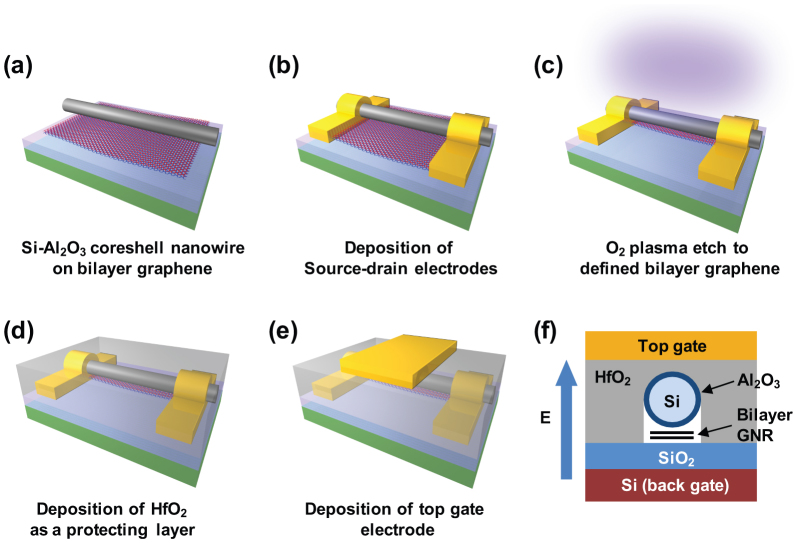
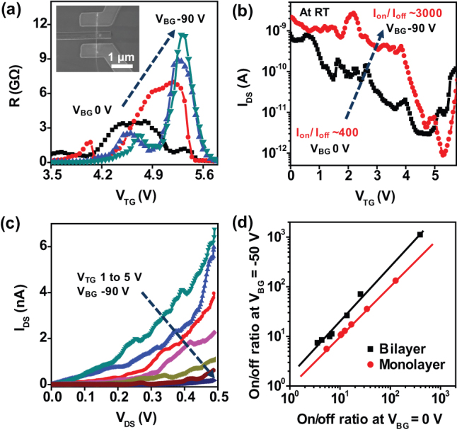
The lack of a bandgap makes bulk graphene unsuitable for room temperature transistors with a sufficient on/off current ratio. Lateral constriction of charge carriers in graphene nanostructures or vertical inversion symmetry breaking in bilayer graphene are two potential strategies to mitigate this challenge, but each alone is insufficient to consistently achieve a large enough on/off ratio (e.g. > 1000) for typical logic applications. Herein we report the combination of lateral carrier constriction and vertical inversion symmetry breaking in bilayer graphene nanoribbons (GNRs) to tune their transport gaps and improve the on/off ratio. Our studies demonstrate that the on/off current ratio of bilayer GNRs can be systematically increased upon applying a vertical electric field, to achieve a largest on/off current ratio over 3000 at room temperature.

摘要

由于缺乏能隙,体石墨烯不适合在室温下用于具有足够导通-截止电流比的晶体管。在石墨烯纳米结构中横向限制电荷载流子或在双层石墨烯中打破垂直反转对称性是两种潜在的策略,可以缓解这一挑战,但单独使用任何一种策略都不足以始终如一地实现足够大的导通-截止电流比(例如,>1000),无法满足典型逻辑应用的要求。在此,我们报告了在双层石墨烯纳米带(GNRs)中结合横向载流子限制和垂直反转对称性破坏来调节其传输能隙并提高导通-截止电流比。我们的研究表明,通过施加垂直电场,双层 GNR 的导通-截止电流比可以系统地增加,从而在室温下实现超过 3000 的最大导通-截止电流比。

https://cdn.ncbi.nlm.nih.gov/pmc/blobs/3b48/3570781/4fbb760d17b1/srep01248-f4.jpg
https://cdn.ncbi.nlm.nih.gov/pmc/blobs/3b48/3570781/b4d7ae78c1ee/srep01248-f1.jpg
https://cdn.ncbi.nlm.nih.gov/pmc/blobs/3b48/3570781/2f1d9c578a5d/srep01248-f2.jpg
https://cdn.ncbi.nlm.nih.gov/pmc/blobs/3b48/3570781/99551b074f99/srep01248-f3.jpg
https://cdn.ncbi.nlm.nih.gov/pmc/blobs/3b48/3570781/4fbb760d17b1/srep01248-f4.jpg

相似文献

1
Tunable transport gap in narrow bilayer graphene nanoribbons.窄双层石墨烯纳米带中的可调谐输运能隙。
Sci Rep. 2013;3:1248. doi: 10.1038/srep01248. Epub 2013 Feb 13.
2
High on/off ratios in bilayer graphene field effect transistors realized by surface dopants.通过表面掺杂实现双层石墨烯场效应晶体管的高导通/关断比。
Nano Lett. 2011 Jul 13;11(7):2640-3. doi: 10.1021/nl200631m. Epub 2011 Jun 20.
3
Toward tunable band gap and tunable dirac point in bilayer graphene with molecular doping.通过分子掺杂实现双层石墨烯的可调带隙和可调狄拉克点。
Nano Lett. 2011 Nov 9;11(11):4759-63. doi: 10.1021/nl2025739. Epub 2011 Oct 10.
4
Magnetic response of conductance peak structure in junction-confined graphene nanoribbons.结限制的石墨烯纳米带中电导峰结构的磁响应。
Nanoscale. 2012 Feb 21;4(4):1138-45. doi: 10.1039/c1nr11056j. Epub 2011 Nov 14.
5
Transport characteristics of multichannel transistors made from densely aligned sub-10 nm half-pitch graphene nanoribbons.由密集排列的亚 10nm 半节距石墨烯纳米带制成的多通道晶体管的传输特性。
ACS Nano. 2012 Nov 27;6(11):9700-10. doi: 10.1021/nn303127y. Epub 2012 Oct 18.
6
Atomic structure of epitaxial graphene sidewall nanoribbons: flat graphene, miniribbons, and the confinement gap.外延石墨烯侧壁纳米带的原子结构:平坦石墨烯、小纳米带和约束间隙。
Nano Lett. 2015 Jan 14;15(1):182-9. doi: 10.1021/nl503352v. Epub 2014 Dec 15.
7
Synthesis of structurally well-defined and liquid-phase-processable graphene nanoribbons.结构明确且可在液相中加工的石墨烯纳米带的合成。
Nat Chem. 2014 Feb;6(2):126-32. doi: 10.1038/nchem.1819. Epub 2013 Dec 8.
8
Single-layer MoS2 transistors.单层 MoS2 晶体管。
Nat Nanotechnol. 2011 Mar;6(3):147-50. doi: 10.1038/nnano.2010.279. Epub 2011 Jan 30.
9
Single step synthesis of graphene nanoribbons by catalyst particle size dependent cutting of multiwalled carbon nanotubes.通过催化剂粒径依赖性切割多壁碳纳米管的单步合成石墨烯纳米带。
Nanoscale. 2011 Sep 1;3(9):3876-82. doi: 10.1039/c1nr10483g. Epub 2011 Aug 15.
10
Sub-10 nm Graphene Nanoribbon Array field-effect transistors fabricated by block copolymer lithography.通过嵌段共聚物光刻技术制备的亚 10nm 石墨烯纳米带阵列场效应晶体管。
Adv Mater. 2013 Sep 14;25(34):4723-8. doi: 10.1002/adma.201300813. Epub 2013 Jun 25.

引用本文的文献

1
A carbon nanotube-graphene nanoribbon seamless junction transistor.一种碳纳米管-石墨烯纳米带无缝结晶体管。
Nanoscale Adv. 2020 Jan 30;2(2):659-663. doi: 10.1039/c9na00797k. eCollection 2020 Feb 18.
2
Dirac cone move and bandgap on/off switching of graphene superlattice.狄拉克锥移动与石墨烯超晶格的带隙开/关切换
Sci Rep. 2016 Jan 6;6:18869. doi: 10.1038/srep18869.
3
Synthesis of quasi-free-standing bilayer graphene nanoribbons on SiC surfaces.在碳化硅表面合成准独立双层石墨烯纳米带。

本文引用的文献

1
Toward tunable band gap and tunable dirac point in bilayer graphene with molecular doping.通过分子掺杂实现双层石墨烯的可调带隙和可调狄拉克点。
Nano Lett. 2011 Nov 9;11(11):4759-63. doi: 10.1021/nl2025739. Epub 2011 Oct 10.
2
Observation of Raman g-peak split for graphene nanoribbons with hydrogen-terminated zigzag edges.观察具有氢终止锯齿边缘的石墨烯纳米带的拉曼 g-峰分裂。
Nano Lett. 2011 Oct 12;11(10):4083-8. doi: 10.1021/nl201387x. Epub 2011 Sep 9.
3
High-frequency, scaled graphene transistors on diamond-like carbon.在类金刚石碳上的高频、可扩展的石墨烯晶体管。
Nat Commun. 2015 Jul 9;6:7632. doi: 10.1038/ncomms8632.
4
Photocurrent generation in lateral graphene p-n junction created by electron-beam irradiation.电子束辐照产生的横向石墨烯p-n结中的光电流生成。
Sci Rep. 2015 Jul 8;5:12014. doi: 10.1038/srep12014.
Nature. 2011 Apr 7;472(7341):74-8. doi: 10.1038/nature09979.
4
High-speed graphene transistors with a self-aligned nanowire gate.具有自对准纳米线栅的高速石墨烯晶体管。
Nature. 2010 Sep 16;467(7313):305-8. doi: 10.1038/nature09405. Epub 2010 Sep 1.
5
Boron nitride substrates for high-quality graphene electronics.氮化硼衬底用于高质量石墨烯电子学。
Nat Nanotechnol. 2010 Oct;5(10):722-6. doi: 10.1038/nnano.2010.172. Epub 2010 Aug 22.
6
Very large magnetoresistance in graphene nanoribbons.石墨烯纳米带中的巨磁电阻
Nat Nanotechnol. 2010 Sep;5(9):655-9. doi: 10.1038/nnano.2010.154. Epub 2010 Aug 8.
7
Etching and narrowing of graphene from the edges.从边缘刻蚀和缩小石墨烯。
Nat Chem. 2010 Aug;2(8):661-5. doi: 10.1038/nchem.719. Epub 2010 Jun 27.
8
Graphene transistors.石墨烯晶体管。
Nat Nanotechnol. 2010 Jul;5(7):487-96. doi: 10.1038/nnano.2010.89. Epub 2010 May 30.
9
Top-gated graphene nanoribbon transistors with ultrathin high-k dielectrics.顶栅石墨烯纳米带晶体管与超薄高介电常数介质
Nano Lett. 2010 May 12;10(5):1917-21. doi: 10.1021/nl100840z.
10
Electron transport in disordered graphene nanoribbons.无序石墨烯纳米带中的电子输运。
Phys Rev Lett. 2010 Feb 5;104(5):056801. doi: 10.1103/PhysRevLett.104.056801. Epub 2010 Feb 1.