• 文献检索
  • 文档翻译
  • 深度研究
  • 学术资讯
  • Suppr Zotero 插件Zotero 插件
  • 邀请有礼
  • 套餐&价格
  • 历史记录
应用&插件
Suppr Zotero 插件Zotero 插件浏览器插件Mac 客户端Windows 客户端微信小程序
定价
高级版会员购买积分包购买API积分包
服务
文献检索文档翻译深度研究API 文档MCP 服务
关于我们
关于 Suppr公司介绍联系我们用户协议隐私条款
关注我们

Suppr 超能文献

核心技术专利:CN118964589B侵权必究
粤ICP备2023148730 号-1Suppr @ 2026

文献检索

告别复杂PubMed语法,用中文像聊天一样搜索,搜遍4000万医学文献。AI智能推荐,让科研检索更轻松。

立即免费搜索

文件翻译

保留排版,准确专业,支持PDF/Word/PPT等文件格式,支持 12+语言互译。

免费翻译文档

深度研究

AI帮你快速写综述,25分钟生成高质量综述,智能提取关键信息,辅助科研写作。

立即免费体验

基于垂直硅纳米线的多光谱成像。

Multispectral imaging with vertical silicon nanowires.

机构信息

School of Engineering and Applied Sciences, Harvard University, Cambridge, Massachusetts 02138, USA.

出版信息

Sci Rep. 2013;3:2460. doi: 10.1038/srep02460.

DOI:10.1038/srep02460
PMID:23955156
原文链接:https://pmc.ncbi.nlm.nih.gov/articles/PMC3746203/
Abstract

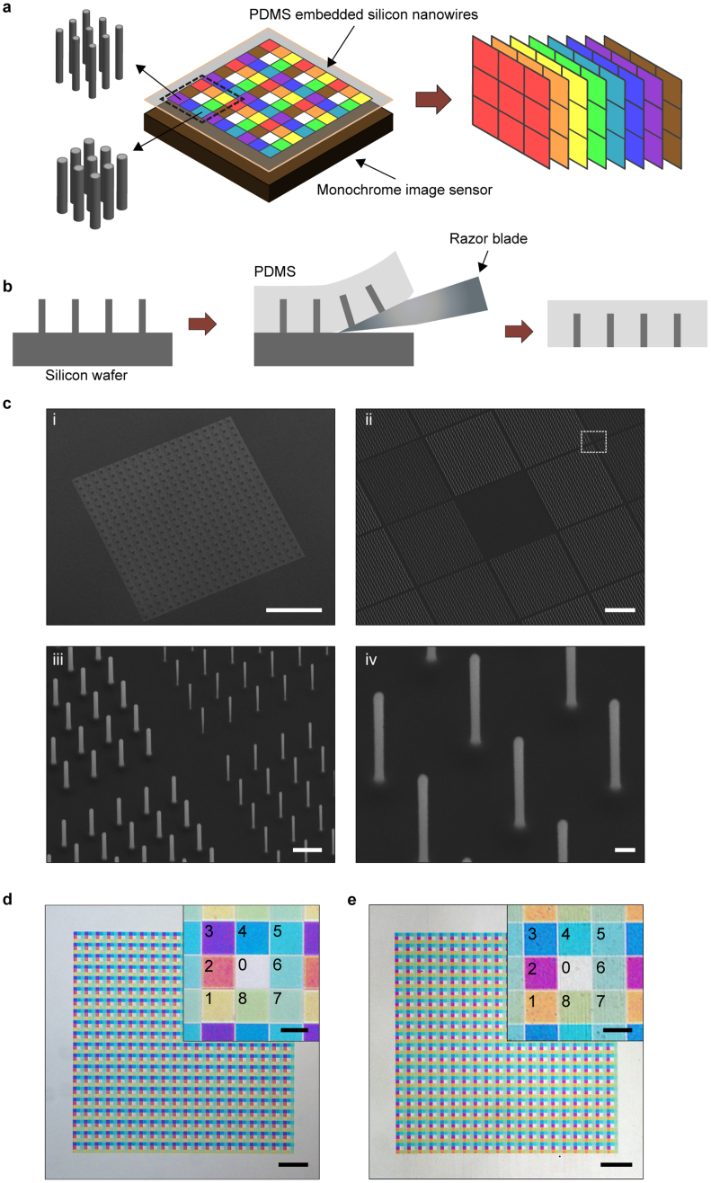
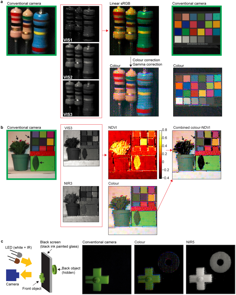
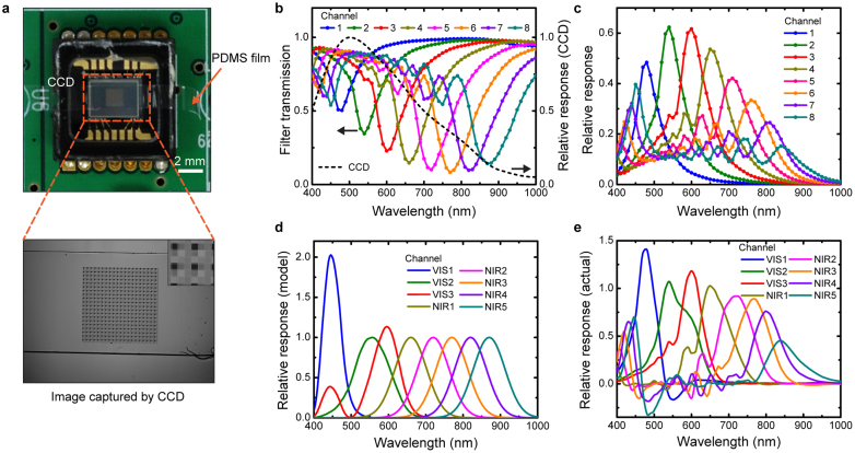
Multispectral imaging is a powerful tool that extends the capabilities of the human eye. However, multispectral imaging systems generally are expensive and bulky, and multiple exposures are needed. Here, we report the demonstration of a compact multispectral imaging system that uses vertical silicon nanowires to realize a filter array. Multiple filter functions covering visible to near-infrared (NIR) wavelengths are simultaneously defined in a single lithography step using a single material (silicon). Nanowires are then etched and embedded into polydimethylsiloxane (PDMS), thereby realizing a device with eight filter functions. By attaching it to a monochrome silicon image sensor, we successfully realize an all-silicon multispectral imaging system. We demonstrate visible and NIR imaging. We show that the latter is highly sensitive to vegetation and furthermore enables imaging through objects opaque to the eye.

摘要

多光谱成像是一种强大的工具,可以扩展人眼的能力。然而,多光谱成像系统通常昂贵且庞大,并且需要多次曝光。在这里,我们报告了一种使用垂直硅纳米线实现滤光片阵列的紧凑型多光谱成像系统的演示。使用单一材料(硅),在单个光刻步骤中同时定义了覆盖可见到近红外(NIR)波长的多个滤光功能。然后对纳米线进行刻蚀并嵌入到聚二甲基硅氧烷(PDMS)中,从而实现具有八个滤光功能的器件。通过将其附着到单色硅图像传感器上,我们成功地实现了全硅多光谱成像系统。我们演示了可见和近红外成像。我们表明,后者对植被非常敏感,并且可以通过人眼无法看到的物体进行成像。

https://cdn.ncbi.nlm.nih.gov/pmc/blobs/702f/3746203/504828d3335e/srep02460-f3.jpg
https://cdn.ncbi.nlm.nih.gov/pmc/blobs/702f/3746203/3e783d2cde73/srep02460-f1.jpg
https://cdn.ncbi.nlm.nih.gov/pmc/blobs/702f/3746203/741a4f591721/srep02460-f2.jpg
https://cdn.ncbi.nlm.nih.gov/pmc/blobs/702f/3746203/504828d3335e/srep02460-f3.jpg
https://cdn.ncbi.nlm.nih.gov/pmc/blobs/702f/3746203/3e783d2cde73/srep02460-f1.jpg
https://cdn.ncbi.nlm.nih.gov/pmc/blobs/702f/3746203/741a4f591721/srep02460-f2.jpg
https://cdn.ncbi.nlm.nih.gov/pmc/blobs/702f/3746203/504828d3335e/srep02460-f3.jpg

相似文献

1
Multispectral imaging with vertical silicon nanowires.基于垂直硅纳米线的多光谱成像。
Sci Rep. 2013;3:2460. doi: 10.1038/srep02460.
2
Nanohole-array-based device for 2D snapshot multispectral imaging.基于纳米孔阵列的二维快照多光谱成像设备。
Sci Rep. 2013;3:2589. doi: 10.1038/srep02589.
3
Tip-enhanced Raman imaging and nano spectroscopy of etched silicon nanowires.硅纳米线的增强拉曼成像和纳米光谱学研究
Sensors (Basel). 2013 Sep 25;13(10):12744-59. doi: 10.3390/s131012744.
4
Interference lithographically defined and catalytically etched, large-area silicon nanocones from nanowires.利用干涉光刻定义并通过催化刻蚀,从纳米线得到大面积硅纳米锥。
Nanotechnology. 2010 May 21;21(20):205305. doi: 10.1088/0957-4484/21/20/205305. Epub 2010 Apr 26.
5
Silicon nanowire biologically sensitive field effect transistors: electrical characteristics and applications.硅纳米线生物敏感场效应晶体管:电学特性及应用
J Nanosci Nanotechnol. 2014 Jan;14(1):273-87. doi: 10.1166/jnn.2014.8760.
6
Silicon nanowire field-effect-transistor based biosensors: from sensitive to ultra-sensitive.基于硅纳米线场效应晶体管的生物传感器:从灵敏到超灵敏。
Biosens Bioelectron. 2014 Oct 15;60:101-11. doi: 10.1016/j.bios.2014.03.057. Epub 2014 Apr 15.
7
Micro-Fresnel-Zone-Plate Array on Flexible Substrate for Large Field-of-View and Focus Scanning.用于大视野和聚焦扫描的柔性基板上的微菲涅耳区板阵列
Sci Rep. 2015 Oct 30;5:15861. doi: 10.1038/srep15861.
8
Origin of visible and near-infrared photoluminescence from chemically etched Si nanowires decorated with arbitrarily shaped Si nanocrystals.化学腐蚀的具有任意形状的硅纳米晶修饰的硅纳米线的可见光和近红外光致发光的起源。
Nanotechnology. 2014 Jan 31;25(4):045703. doi: 10.1088/0957-4484/25/4/045703. Epub 2014 Jan 6.
9
Silicon nanowire circuits fabricated by AFM oxidation nanolithography.原子力显微镜氧化刻蚀技术制备的硅纳米线电路。
Nanotechnology. 2010 Jun 18;21(24):245301. doi: 10.1088/0957-4484/21/24/245301. Epub 2010 May 20.
10
Optical Transduction for Vertical Nanowire Resonators.垂直纳米线谐振器的光转换。
Nano Lett. 2020 Apr 8;20(4):2359-2369. doi: 10.1021/acs.nanolett.9b04909. Epub 2020 Mar 25.

引用本文的文献

1
Trends in Snapshot Spectral Imaging: Systems, Processing, and Quality.快照光谱成像的趋势:系统、处理与质量
Sensors (Basel). 2025 Jan 23;25(3):675. doi: 10.3390/s25030675.
2
Single Seed Identification in Three Species via Multispectral Imaging Combined with Stacking Ensemble Learning.基于多光谱成像与堆叠集成学习的三种物种单粒种子鉴别。
Sensors (Basel). 2022 Oct 4;22(19):7521. doi: 10.3390/s22197521.
3
A Spectral Filter Array Camera for Clinical Monitoring and Diagnosis: Proof of Concept for Skin Oxygenation Imaging.用于临床监测与诊断的光谱滤波阵列相机:皮肤氧合成像的概念验证

本文引用的文献

1
Plasmonic color filters for CMOS image sensor applications.用于 CMOS 图像传感器应用的等离子体颜色滤波器。
Nano Lett. 2012 Aug 8;12(8):4349-54. doi: 10.1021/nl302110z. Epub 2012 Jul 17.
2
Multicolored vertical silicon nanowires.多色垂直硅纳米线。
Nano Lett. 2011 Apr 13;11(4):1851-6. doi: 10.1021/nl200201b. Epub 2011 Mar 17.
3
Plasmonic nanoresonators for high-resolution colour filtering and spectral imaging.等离子体纳米谐振器用于高分辨率颜色滤波和光谱成像。
J Imaging. 2019 Jul 26;5(8):66. doi: 10.3390/jimaging5080066.
4
Optically transparent vertical silicon nanowire arrays for live-cell imaging.用于活细胞成像的光学透明垂直硅纳米线阵列。
J Nanobiotechnology. 2021 Feb 17;19(1):51. doi: 10.1186/s12951-021-00795-7.
5
Nanowire Waveguides and Lasers: Advances and Opportunities in Photonic Circuits.纳米线波导与激光器:光子电路的进展与机遇
Front Chem. 2021 Jan 8;8:613504. doi: 10.3389/fchem.2020.613504. eCollection 2020.
6
Recent Advances in Vertically Aligned Nanowires for Photonics Applications.用于光子学应用的垂直排列纳米线的最新进展
Micromachines (Basel). 2020 Jul 26;11(8):726. doi: 10.3390/mi11080726.
7
Ultrahigh resolution and color gamut with scattering-reducing transmissive pixels.超高分辨率和色域,采用减少散射的透光像素。
Nat Commun. 2019 Oct 21;10(1):4782. doi: 10.1038/s41467-019-12689-2.
8
Recent Applications of Multispectral Imaging in Seed Phenotyping and Quality Monitoring-An Overview.多光谱成像在种子表型和质量监测中的最新应用概述。
Sensors (Basel). 2019 Mar 4;19(5):1090. doi: 10.3390/s19051090.
9
Reflective color filter with precise control of the color coordinate achieved by stacking silicon nanowire arrays onto ultrathin optical coatings.通过将硅纳米线阵列堆叠在超薄光学涂层上实现颜色坐标精确控制的反射式滤色器。
Sci Rep. 2019 Mar 4;9(1):3350. doi: 10.1038/s41598-019-40001-1.
10
Plasmonic- and dielectric-based structural coloring: from fundamentals to practical applications.基于表面等离子体激元和电介质的结构色:从基础到实际应用
Nano Converg. 2018;5(1):1. doi: 10.1186/s40580-017-0133-y. Epub 2018 Jan 10.
Nat Commun. 2010 Aug 24;1:59. doi: 10.1038/ncomms1058.
4
Tuning the color of silicon nanostructures.硅纳米结构的颜色调控。
Nano Lett. 2010 Jul 14;10(7):2649-54. doi: 10.1021/nl1013794.
5
Three-dimensional nanopillar-array photovoltaics on low-cost and flexible substrates.基于低成本柔性衬底的三维纳米柱阵列光伏器件
Nat Mater. 2009 Aug;8(8):648-53. doi: 10.1038/nmat2493. Epub 2009 Jul 5.
6
A hemispherical electronic eye camera based on compressible silicon optoelectronics.基于可压缩硅光电子学的半球形电子眼相机。
Nature. 2008 Aug 7;454(7205):748-53. doi: 10.1038/nature07113.
7
Multispectral imaging in biology and medicine: slices of life.生物学与医学中的多光谱成像:生命切片
Cytometry A. 2006 Aug 1;69(8):748-58. doi: 10.1002/cyto.a.20319.
8
Pancam multispectral imaging results from the Opportunity Rover at Meridiani Planum.机遇号火星车在子午线平原的全景相机多光谱成像结果。
Science. 2004 Dec 3;306(5702):1703-9. doi: 10.1126/science.1105245.
9
Integrated color pixels in 0.18-microm complementary metal oxide semiconductor technology.采用0.18微米互补金属氧化物半导体技术的集成彩色像素。
J Opt Soc Am A Opt Image Sci Vis. 2003 Dec;20(12):2293-306. doi: 10.1364/josaa.20.002293.