• 文献检索
  • 文档翻译
  • 深度研究
  • 学术资讯
  • Suppr Zotero 插件Zotero 插件
  • 邀请有礼
  • 套餐&价格
  • 历史记录
应用&插件
Suppr Zotero 插件Zotero 插件浏览器插件Mac 客户端Windows 客户端微信小程序
定价
高级版会员购买积分包购买API积分包
服务
文献检索文档翻译深度研究API 文档MCP 服务
关于我们
关于 Suppr公司介绍联系我们用户协议隐私条款
关注我们

Suppr 超能文献

核心技术专利:CN118964589B侵权必究
粤ICP备2023148730 号-1Suppr @ 2026

文献检索

告别复杂PubMed语法,用中文像聊天一样搜索,搜遍4000万医学文献。AI智能推荐,让科研检索更轻松。

立即免费搜索

文件翻译

保留排版,准确专业,支持PDF/Word/PPT等文件格式,支持 12+语言互译。

免费翻译文档

深度研究

AI帮你快速写综述,25分钟生成高质量综述,智能提取关键信息,辅助科研写作。

立即免费体验

温度触发的面内和面内垂直堆叠的石墨烯-氮化硼异质结构的化学转换生长

Temperature-triggered chemical switching growth of in-plane and vertically stacked graphene-boron nitride heterostructures.

作者信息

Gao Teng, Song Xiuju, Du Huiwen, Nie Yufeng, Chen Yubin, Ji Qingqing, Sun Jingyu, Yang Yanlian, Zhang Yanfeng, Liu Zhongfan

机构信息

Center for Nanochemistry (CNC), Beijing Science and Engineering Center for Low-Dimensional Carbon Materials, Beijing National Laboratory for Molecular Sciences, College of Chemistry and Molecular Engineering, Peking University, Beijing 100871, China.

National Center for Nanoscience and Technology, Beijing 100190, China.

出版信息

Nat Commun. 2015 Apr 14;6:6835. doi: 10.1038/ncomms7835.

DOI:10.1038/ncomms7835
PMID:25869236
原文链接:https://pmc.ncbi.nlm.nih.gov/articles/PMC4403442/
Abstract

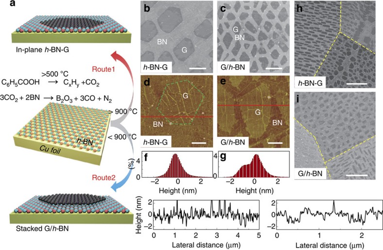
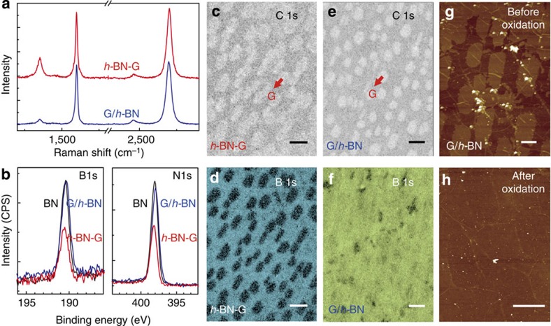
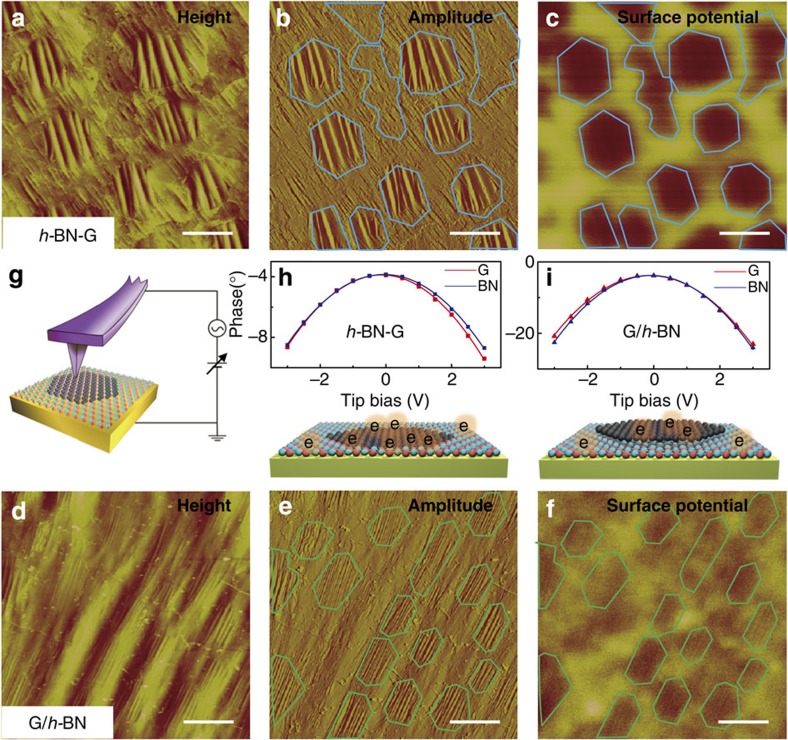
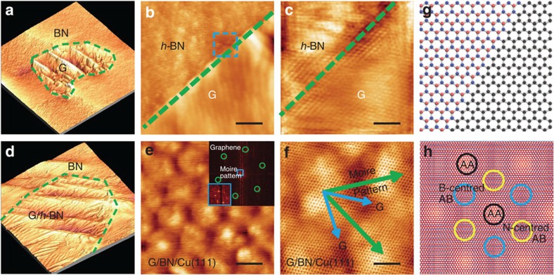
In-plane and vertically stacked heterostructures of graphene and hexagonal boron nitride (h-BN-G and G/h-BN, respectively) are both recent focuses of graphene research. However, targeted synthesis of either heterostructure remains a challenge. Here, via chemical vapour deposition and using benzoic acid precursor, we have achieved the selective growth of h-BN-G and G/h-BN through a temperature-triggered switching reaction. The perfect in-plane h-BN-G is characterized by scanning tunnelling microscopy (STM), showing atomically patched graphene and h-BN with typical zigzag edges. In contrast, the vertical alignment of G/h-BN is confirmed by unique lattice-mismatch-induced moiré patterns in high-resolution STM images, and two sets of aligned selected area electron diffraction spots, both suggesting a van der Waals epitaxial mechanism. The present work demonstrates the chemical designability of growth process for controlled synthesis of graphene and h-BN heterostructures. With practical scalability, high uniformity and quality, our approach will promote the development of graphene-based electronics and optoelectronics.

摘要

石墨烯与六方氮化硼的面内及垂直堆叠异质结构(分别为h-BN-G和G/h-BN)均是近期石墨烯研究的重点。然而,有针对性地合成这两种异质结构仍然是一项挑战。在此,通过化学气相沉积法并使用苯甲酸前驱体,我们通过温度触发的切换反应实现了h-BN-G和G/h-BN的选择性生长。完美的面内h-BN-G通过扫描隧道显微镜(STM)进行表征,显示出原子级拼接的石墨烯和具有典型锯齿形边缘的h-BN。相比之下,G/h-BN的垂直排列通过高分辨率STM图像中独特的晶格失配诱导的莫尔条纹以及两组对齐的选区电子衍射斑点得以证实,这两者均表明存在范德华外延机制。本工作展示了用于可控合成石墨烯和h-BN异质结构的生长过程的化学可设计性。凭借实际可扩展性、高均匀性和高质量,我们的方法将推动基于石墨烯的电子学和光电子学的发展。

https://cdn.ncbi.nlm.nih.gov/pmc/blobs/c0e4/4403442/b722916b6533/ncomms7835-f5.jpg
https://cdn.ncbi.nlm.nih.gov/pmc/blobs/c0e4/4403442/b6bd5ce49329/ncomms7835-f1.jpg
https://cdn.ncbi.nlm.nih.gov/pmc/blobs/c0e4/4403442/c4a8e736a7af/ncomms7835-f2.jpg
https://cdn.ncbi.nlm.nih.gov/pmc/blobs/c0e4/4403442/e31c03c8223d/ncomms7835-f3.jpg
https://cdn.ncbi.nlm.nih.gov/pmc/blobs/c0e4/4403442/c01cb95db455/ncomms7835-f4.jpg
https://cdn.ncbi.nlm.nih.gov/pmc/blobs/c0e4/4403442/b722916b6533/ncomms7835-f5.jpg

相似文献

1
Temperature-triggered chemical switching growth of in-plane and vertically stacked graphene-boron nitride heterostructures.温度触发的面内和面内垂直堆叠的石墨烯-氮化硼异质结构的化学转换生长
Nat Commun. 2015 Apr 14;6:6835. doi: 10.1038/ncomms7835.
2
Hexagonal Boron Nitride-Graphene Heterostructures: Synthesis and Interfacial Properties.六方氮化硼-石墨烯杂化结构:合成与界面性质。
Small. 2016 Jan 6;12(1):32-50. doi: 10.1002/smll.201501766. Epub 2015 Oct 6.
3
Synthesis of in-plane and stacked graphene/hexagonal boron nitride heterostructures by combining with ion beam sputtering deposition and chemical vapor deposition.通过结合离子束溅射沉积和化学气相沉积合成面内和堆叠的石墨烯/六方氮化硼异质结构。
Nanoscale. 2015 Oct 14;7(38):16046-53. doi: 10.1039/c5nr04490a. Epub 2015 Sep 15.
4
Direct growth of large-area graphene and boron nitride heterostructures by a co-segregation method.通过共偏析方法直接生长大面积石墨烯和氮化硼异质结。
Nat Commun. 2015 Mar 4;6:6519. doi: 10.1038/ncomms7519.
5
Nickelocene-Precursor-Facilitated Fast Growth of Graphene/h-BN Vertical Heterostructures and Its Applications in OLEDs.镍夹心配合物促进石墨烯/六方氮化硼垂直异质结构的快速生长及其在 OLEDs 中的应用。
Adv Mater. 2017 Aug;29(32). doi: 10.1002/adma.201701325. Epub 2017 Jun 20.
6
Atomically Sharp Interface in an h-BN-epitaxial graphene van der Waals Heterostructure.六方氮化硼外延石墨烯范德华异质结构中的原子级尖锐界面
Sci Rep. 2015 Nov 20;5:16465. doi: 10.1038/srep16465.
7
A hybrid MBE-based growth method for large-area synthesis of stacked hexagonal boron nitride/graphene heterostructures.基于 MBE 的混合生长法用于大面积合成堆叠六方氮化硼/石墨烯异质结。
Sci Rep. 2017 Feb 27;7:43644. doi: 10.1038/srep43644.
8
Epitaxial chemical vapour deposition growth of monolayer hexagonal boron nitride on a Cu(111)/sapphire substrate.在Cu(111)/蓝宝石衬底上进行单层六方氮化硼的外延化学气相沉积生长。
Phys Chem Chem Phys. 2017 Mar 22;19(12):8230-8235. doi: 10.1039/c6cp08903h.
9
In-situ epitaxial growth of graphene/h-BN van der Waals heterostructures by molecular beam epitaxy.通过分子束外延法原位外延生长石墨烯/h-BN范德华异质结构
Sci Rep. 2015 Oct 7;5:14760. doi: 10.1038/srep14760.
10
Synthesis of High-Quality Graphene and Hexagonal Boron Nitride Monolayer In-Plane Heterostructure on Cu-Ni Alloy.在铜镍合金上合成高质量石墨烯和六方氮化硼单层面内异质结构
Adv Sci (Weinh). 2017 May 19;4(9):1700076. doi: 10.1002/advs.201700076. eCollection 2017 Sep.

引用本文的文献

1
Interface-Enhanced and Self-Guided Growth of 2D Interlayer Heterostructure Wafers with Vertically Aligned Van Der Waals Layers.具有垂直排列范德华层的二维层间异质结构晶圆的界面增强与自引导生长
Adv Sci (Weinh). 2025 Apr;12(14):e2412690. doi: 10.1002/advs.202412690. Epub 2025 Feb 17.
2
Non-volatile 2D MoS/black phosphorus heterojunction photodiodes in the near- to mid-infrared region.近红外至中红外区域的非易失性二维MoS/黑磷异质结光电二极管。
Nat Commun. 2024 Jul 17;15(1):6015. doi: 10.1038/s41467-024-50353-6.
3
1D and 2D Boron Nitride Nano Structures: A Critical Analysis for Emerging Applications in the Field of Nanocomposites.

本文引用的文献

1
Spatially resolved one-dimensional boundary states in graphene-hexagonal boron nitride planar heterostructures.石墨烯-六方氮化硼平面异质结中的一维局域边界态。
Nat Commun. 2014 Nov 7;5:5403. doi: 10.1038/ncomms6403.
2
Quasi-freestanding monolayer heterostructure of graphene and hexagonal boron nitride on Ir(111) with a zigzag boundary.在 Ir(111)上具有锯齿形边界的准自由-standing 单层石墨烯和六方氮化硼杂化结构。
Nano Lett. 2014 Nov 12;14(11):6342-7. doi: 10.1021/nl502780u. Epub 2014 Oct 8.
3
Electronic states at the graphene-hexagonal boron nitride zigzag interface.
一维和二维氮化硼纳米结构:对纳米复合材料领域新兴应用的批判性分析
ACS Omega. 2024 Jun 12;9(25):26737-26761. doi: 10.1021/acsomega.3c10217. eCollection 2024 Jun 25.
4
Continuous orientated growth of scaled single-crystal 2D monolayer films.规模化单晶二维单层膜的连续定向生长。
Nanoscale Adv. 2021 Oct 29;3(23):6545-6567. doi: 10.1039/d1na00545f. eCollection 2021 Nov 24.
5
Methods of hexagonal boron nitride exfoliation and its functionalization: covalent and non-covalent approaches.六方氮化硼的剥离方法及其功能化:共价和非共价方法。
RSC Adv. 2021 Sep 23;11(50):31284-31327. doi: 10.1039/d1ra05727h. eCollection 2021 Sep 21.
6
Defects in graphene-based heterostructures: topological and geometrical effects.基于石墨烯的异质结构中的缺陷:拓扑和几何效应。
RSC Adv. 2022 Feb 28;12(11):6772-6782. doi: 10.1039/d1ra08884j. eCollection 2022 Feb 22.
7
Tuning adlayer-substrate interactions of graphene/h-BN heterostructures on Cu(111)-Ni and Ni(111)-Cu surface alloys.调控石墨烯/h-BN异质结构在Cu(111)-Ni和Ni(111)-Cu表面合金上的吸附层-衬底相互作用
RSC Adv. 2021 Jan 6;11(4):1916-1927. doi: 10.1039/d0ra08622c.
8
Epitaxy of 2D Materials toward Single Crystals.二维材料向单晶的外延生长。
Adv Sci (Weinh). 2022 Mar;9(8):e2105201. doi: 10.1002/advs.202105201. Epub 2022 Jan 17.
9
Direct growth of hexagonal boron nitride on non-metallic substrates and its heterostructures with graphene.六方氮化硼在非金属衬底上的直接生长及其与石墨烯的异质结构
iScience. 2021 Oct 28;24(11):103374. doi: 10.1016/j.isci.2021.103374. eCollection 2021 Nov 19.
10
Defects in Graphene/h-BN Planar Heterostructures: Insights into the Interfacial Thermal Transport Properties.石墨烯/六方氮化硼平面异质结构中的缺陷:对界面热输运性质的洞察
Nanomaterials (Basel). 2021 Feb 16;11(2):500. doi: 10.3390/nano11020500.
石墨烯-六方氮化硼锯齿界面的电子态。
Nano Lett. 2014 Sep 10;14(9):5128-32. doi: 10.1021/nl501895h. Epub 2014 Aug 5.
4
Nanoscale integration of two-dimensional materials by lateral heteroepitaxy.二维材料的横向异质外延纳尺度集成。
Nano Lett. 2014 Aug 13;14(8):4846-51. doi: 10.1021/nl502110q. Epub 2014 Jul 28.
5
Catalytic transparency of hexagonal boron nitride on copper for chemical vapor deposition growth of large-area and high-quality graphene.六方氮化硼在铜上的催化透明性用于大面积高质量石墨烯的化学气相沉积生长。
ACS Nano. 2014 Jun 24;8(6):5478-83. doi: 10.1021/nn501837c. Epub 2014 Jun 2.
6
Heteroepitaxial growth of two-dimensional hexagonal boron nitride templated by graphene edges.石墨烯边缘模板二维六方氮化硼的异质外延生长。
Science. 2014 Jan 10;343(6167):163-7. doi: 10.1126/science.1246137.
7
Monolayer hexagonal boron nitride films with large domain size and clean interface for enhancing the mobility of graphene-based field-effect transistors.用于提高基于石墨烯的场效应晶体管迁移率的大畴尺寸和清洁界面的单层六方氮化硼薄膜。
Adv Mater. 2014 Mar 12;26(10):1559-64. doi: 10.1002/adma.201304937. Epub 2013 Dec 17.
8
Continuous growth of hexagonal graphene and boron nitride in-plane heterostructures by atmospheric pressure chemical vapor deposition.常压化学气相沉积法连续生长六方石墨烯和氮化硼面内异质结。
ACS Nano. 2013 Nov 26;7(11):10129-38. doi: 10.1021/nn404331f. Epub 2013 Nov 13.
9
Epitaxial growth of single-domain graphene on hexagonal boron nitride.在六方氮化硼上外延生长单畴石墨烯。
Nat Mater. 2013 Sep;12(9):792-7. doi: 10.1038/nmat3695. Epub 2013 Jul 14.
10
Toward single-layer uniform hexagonal boron nitride-graphene patchworks with zigzag linking edges.具有锯齿形连接边缘的单层均匀六方氮化硼-石墨烯拼接。
Nano Lett. 2013 Jul 10;13(7):3439-43. doi: 10.1021/nl4021123. Epub 2013 Jun 14.