Leitao Diana C, Coelho Paulo, Borme Jerome, Knudde Simon, Cardoso Susana, Freitas Paulo P
INESC-MN - Instituto de Engenharia de Sistemas e Computadores - Microsistemas e Nanotecnologias and IN - Institute of Nanoscience and Nanotechnology, Rua Alves Redol 9, Lisboa 1000-029, Portugal.
Instituto Superior Técnico, Universidade de Lisboa, Av. Rovisco Pais, Lisboa 1000, Portugal.
Sensors (Basel). 2015 Dec 4;15(12):30311-8. doi: 10.3390/s151229809.
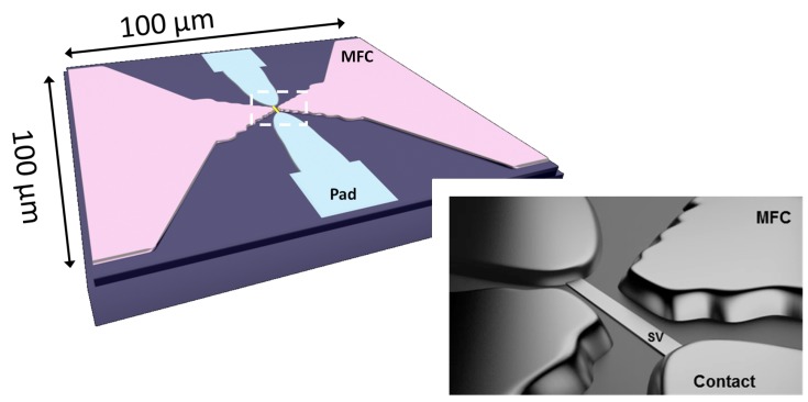
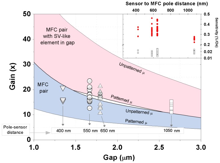
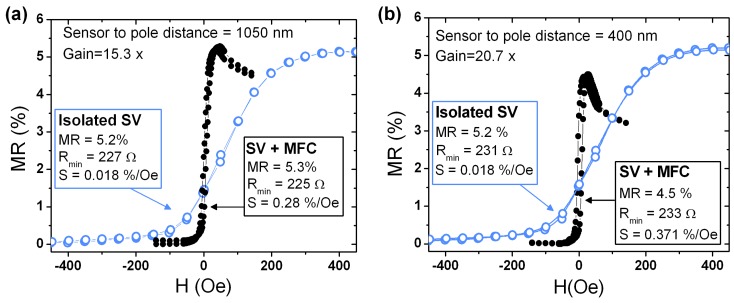
Magnetic field mapping with micrometric spatial resolution and high sensitivity is a challenging application, and the technological solutions are usually based on large area devices integrating discrete magnetic flux guide elements. In this work we demonstrate a high performance hybrid device with improved field sensitivity levels and small footprint, consisting of a ultra-compact 2D design where nanometric spin valve sensors are inserted within the gap of thin-film magnetic flux concentrators. Pole-sensor distances down to 400 nm are demonstrated using nanofabrication techniques combined with an optimized liftoff process. These 100 × 100 μm2 pixel sensors can be integrated in modular devices for surface mapping without moving parts.
具有微米级空间分辨率和高灵敏度的磁场测绘是一项具有挑战性的应用,其技术解决方案通常基于集成离散磁通量引导元件的大面积设备。在这项工作中,我们展示了一种高性能混合设备,其具有更高的场灵敏度水平和更小的占地面积,该设备采用超紧凑二维设计,其中纳米级自旋阀传感器插入薄膜磁通量集中器的间隙中。使用纳米制造技术结合优化的剥离工艺,展示了低至400 nm的磁极-传感器距离。这些100×100μm2像素传感器可以集成到模块化设备中,用于无需移动部件的表面测绘。