• 文献检索
  • 文档翻译
  • 深度研究
  • 学术资讯
  • Suppr Zotero 插件Zotero 插件
  • 邀请有礼
  • 套餐&价格
  • 历史记录
应用&插件
Suppr Zotero 插件Zotero 插件浏览器插件Mac 客户端Windows 客户端微信小程序
定价
高级版会员购买积分包购买API积分包
服务
文献检索文档翻译深度研究API 文档MCP 服务
关于我们
关于 Suppr公司介绍联系我们用户协议隐私条款
关注我们

Suppr 超能文献

核心技术专利:CN118964589B侵权必究
粤ICP备2023148730 号-1Suppr @ 2026

文献检索

告别复杂PubMed语法,用中文像聊天一样搜索,搜遍4000万医学文献。AI智能推荐,让科研检索更轻松。

立即免费搜索

文件翻译

保留排版,准确专业,支持PDF/Word/PPT等文件格式,支持 12+语言互译。

免费翻译文档

深度研究

AI帮你快速写综述,25分钟生成高质量综述,智能提取关键信息,辅助科研写作。

立即免费体验

裸石墨烯和封装石墨烯的近场光电流纳米显微镜技术

Near-field photocurrent nanoscopy on bare and encapsulated graphene.

作者信息

Woessner Achim, Alonso-González Pablo, Lundeberg Mark B, Gao Yuanda, Barrios-Vargas Jose E, Navickaite Gabriele, Ma Qiong, Janner Davide, Watanabe Kenji, Cummings Aron W, Taniguchi Takashi, Pruneri Valerio, Roche Stephan, Jarillo-Herrero Pablo, Hone James, Hillenbrand Rainer, Koppens Frank H L

机构信息

ICFO-Institut de Ciencies Fotoniques, The Barcelona Institute of Science and Technology, 08860 Barcelona, Spain.

CIC nanoGUNE, 20018 Donostia-San Sebastian, Spain.

出版信息

Nat Commun. 2016 Feb 26;7:10783. doi: 10.1038/ncomms10783.

DOI:10.1038/ncomms10783
PMID:26916951
原文链接:https://pmc.ncbi.nlm.nih.gov/articles/PMC4773437/
Abstract

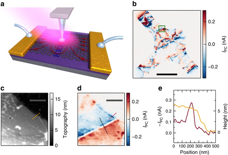
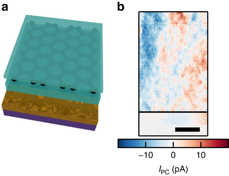
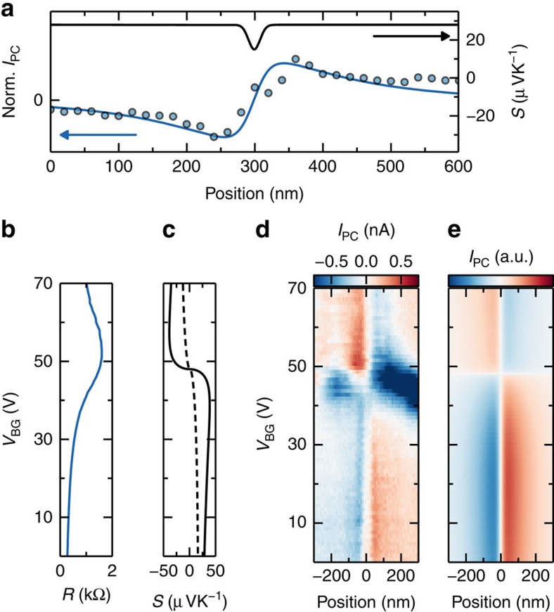
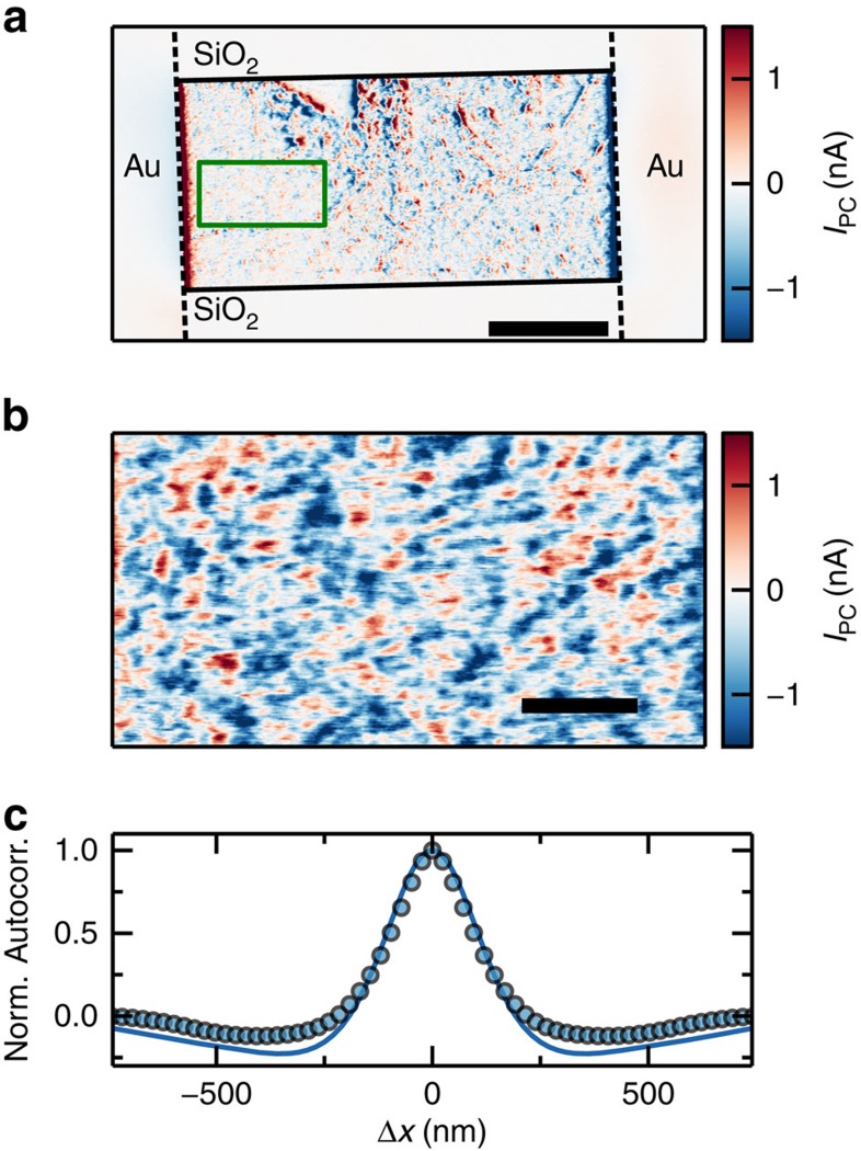
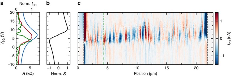
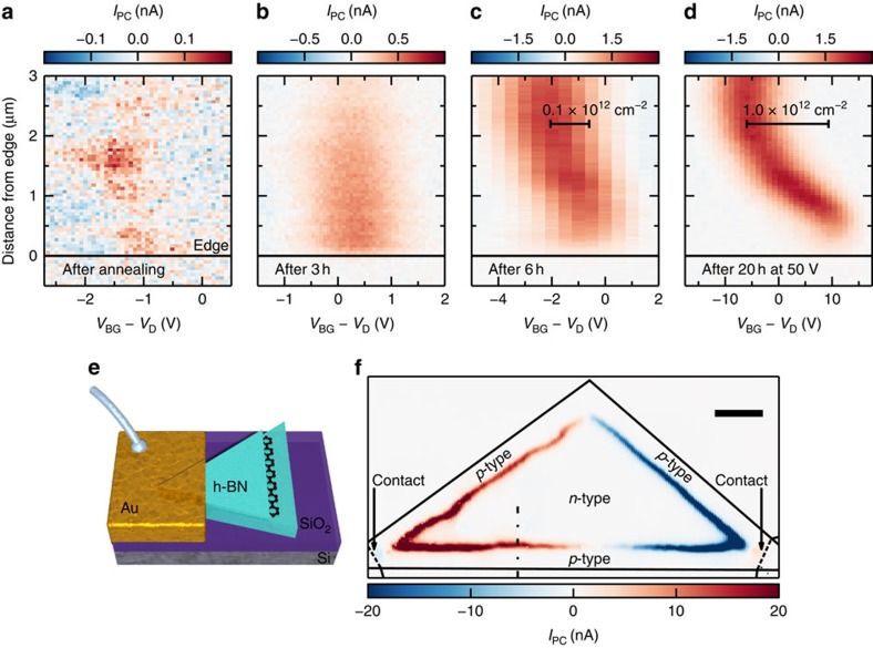
Optoelectronic devices utilizing graphene have demonstrated unique capabilities and performances beyond state-of-the-art technologies. However, requirements in terms of device quality and uniformity are demanding. A major roadblock towards high-performance devices are nanoscale variations of the graphene device properties, impacting their macroscopic behaviour. Here we present and apply non-invasive optoelectronic nanoscopy to measure the optical and electronic properties of graphene devices locally. This is achieved by combining scanning near-field infrared nanoscopy with electrical read-out, allowing infrared photocurrent mapping at length scales of tens of nanometres. Using this technique, we study the impact of edges and grain boundaries on the spatial carrier density profiles and local thermoelectric properties. Moreover, we show that the technique can readily be applied to encapsulated graphene devices. We observe charge build-up near the edges and demonstrate a solution to this issue.

摘要

利用石墨烯的光电器件已展现出超越现有技术的独特能力和性能。然而,对器件质量和均匀性的要求很高。高性能器件面临的一个主要障碍是石墨烯器件特性的纳米级变化,这会影响其宏观行为。在此,我们展示并应用非侵入式光电纳米显微镜来局部测量石墨烯器件的光学和电学性质。这是通过将扫描近场红外纳米显微镜与电学读出相结合来实现的,从而能够在几十纳米的长度尺度上进行红外光电流映射。利用这项技术,我们研究了边缘和晶界对空间载流子密度分布以及局部热电性质的影响。此外,我们表明该技术可以很容易地应用于封装的石墨烯器件。我们观察到边缘附近的电荷积累,并展示了针对此问题的解决方案。

https://cdn.ncbi.nlm.nih.gov/pmc/blobs/94c4/4773437/7dc429be1b52/ncomms10783-f6.jpg
https://cdn.ncbi.nlm.nih.gov/pmc/blobs/94c4/4773437/2a1503772243/ncomms10783-f1.jpg
https://cdn.ncbi.nlm.nih.gov/pmc/blobs/94c4/4773437/0f8645cf93b7/ncomms10783-f2.jpg
https://cdn.ncbi.nlm.nih.gov/pmc/blobs/94c4/4773437/ca858b459ad2/ncomms10783-f3.jpg
https://cdn.ncbi.nlm.nih.gov/pmc/blobs/94c4/4773437/b45e16b57a73/ncomms10783-f4.jpg
https://cdn.ncbi.nlm.nih.gov/pmc/blobs/94c4/4773437/7ecee1ed41f0/ncomms10783-f5.jpg
https://cdn.ncbi.nlm.nih.gov/pmc/blobs/94c4/4773437/7dc429be1b52/ncomms10783-f6.jpg

相似文献

1
Near-field photocurrent nanoscopy on bare and encapsulated graphene.裸石墨烯和封装石墨烯的近场光电流纳米显微镜技术
Nat Commun. 2016 Feb 26;7:10783. doi: 10.1038/ncomms10783.
2
Nano-photocurrent Mapping of Local Electronic Structure in Twisted Bilayer Graphene.扭曲双层石墨烯中局部电子结构的纳米光电流映射
Nano Lett. 2020 May 13;20(5):2958-2964. doi: 10.1021/acs.nanolett.9b04637. Epub 2020 Apr 3.
3
Acoustic terahertz graphene plasmons revealed by photocurrent nanoscopy.声子太赫兹石墨烯等离激元的光电流纳米分辨成像研究
Nat Nanotechnol. 2017 Jan;12(1):31-35. doi: 10.1038/nnano.2016.185. Epub 2016 Oct 24.
4
Simultaneous topographical, electrical and optical microscopy of optoelectronic devices at the nanoscale.纳米尺度下光电设备的形貌、电学和光学显微镜的同步观察。
Nanoscale. 2017 Feb 23;9(8):2723-2731. doi: 10.1039/c6nr09057e.
5
Focused-laser-enabled p-n junctions in graphene field-effect transistors.在石墨烯场效应晶体管中利用聚焦激光实现 p-n 结。
ACS Nano. 2013 Jul 23;7(7):5850-7. doi: 10.1021/nn402354j. Epub 2013 Jun 21.
6
Mapping of Bernal and non-Bernal stacking domains in bilayer graphene using infrared nanoscopy.利用红外纳米光谱技术对双层石墨烯中的伯纳尔和非伯纳尔堆叠畴进行映射。
Nanoscale. 2017 Mar 23;9(12):4191-4195. doi: 10.1039/c7nr00713b.
7
Regulating infrared photoresponses in reduced graphene oxide phototransistors by defect and atomic structure control.通过缺陷和原子结构控制调节还原氧化石墨烯光电晶体管中的红外光响应。
ACS Nano. 2013 Jul 23;7(7):6310-20. doi: 10.1021/nn4023679. Epub 2013 Jun 21.
8
monitoring of electrical and optoelectronic properties of suspended graphene ribbons during laser-induced morphological changes.在激光诱导形态变化过程中对悬浮石墨烯带的电学和光电特性进行监测。
Nanoscale Adv. 2020 Jul 17;2(9):4034-4040. doi: 10.1039/d0na00413h. eCollection 2020 Sep 16.
9
Stacking Structures of Few-Layer Graphene Revealed by Phase-Sensitive Infrared Nanoscopy.层状少层石墨烯的结构通过相敏红外纳米显微镜揭示。
ACS Nano. 2015 Jul 28;9(7):6765-73. doi: 10.1021/acsnano.5b02813. Epub 2015 Jun 15.
10
High Performance Graphene Nano-ribbon Thermoelectric Devices by Incorporation and Dimensional Tuning of Nanopores.通过纳米孔的引入和尺寸调控制备高性能石墨烯纳米带热电器件。
Sci Rep. 2015 Jun 17;5:11297. doi: 10.1038/srep11297.

引用本文的文献

1
Deciphering photocurrent mechanisms at the nanoscale in van der Waals interfaces for enhanced optoelectronic applications.解析范德华界面纳米尺度下的光电流机制以增强光电子应用
Sci Adv. 2025 Aug;11(31):eadv7614. doi: 10.1126/sciadv.adv7614. Epub 2025 Jul 30.
2
Current-driven nonequilibrium electrodynamics in graphene revealed by nano-infrared imaging.通过纳米红外成像揭示的石墨烯中电流驱动的非平衡电动力学
Nat Commun. 2025 Apr 24;16(1):3861. doi: 10.1038/s41467-025-58953-6.
3
Landauer Resistivity Dipole at One-Dimensional Defect Revealed via near-Field Photocurrent Nanoscopy.

本文引用的文献

1
Bimodal Phonon Scattering in Graphene Grain Boundaries.石墨烯晶界中的双模态声子散射。
Nano Lett. 2015 Jul 8;15(7):4532-40. doi: 10.1021/acs.nanolett.5b01100. Epub 2015 Jun 8.
2
Hot-carrier photocurrent effects at graphene-metal interfaces.
J Phys Condens Matter. 2015 Apr 29;27(16):164207. doi: 10.1088/0953-8984/27/16/164207. Epub 2015 Apr 2.
3
Science and technology roadmap for graphene, related two-dimensional crystals, and hybrid systems.石墨烯、相关二维晶体及混合系统的科技路线图。
通过近场光电流纳米显微镜揭示一维缺陷处的朗道尔电阻率偶极子
Nano Lett. 2025 May 28;25(21):8495-8502. doi: 10.1021/acs.nanolett.5c00437. Epub 2025 Apr 10.
4
Metasurface-enabled broadband multidimensional photodetectors.基于超表面的宽带多维光电探测器。
Nat Commun. 2024 Sep 27;15(1):8347. doi: 10.1038/s41467-024-52632-8.
5
Near-field detection of gate-tunable anisotropic plasmon polaritons in black phosphorus at terahertz frequencies.太赫兹频率下黑磷中栅极可调谐各向异性表面等离激元极化激元的近场探测
Nat Commun. 2024 Mar 15;15(1):2373. doi: 10.1038/s41467-024-45264-5.
6
Supercurrent mediated by helical edge modes in bilayer graphene.双层石墨烯中螺旋边缘态介导的超电流。
Nat Commun. 2024 Jan 29;15(1):856. doi: 10.1038/s41467-024-44952-6.
7
Visualizing moiré ferroelectricity via plasmons and nano-photocurrent in graphene/twisted-WSe structures.通过石墨烯/扭曲-WSe结构中的等离激元和纳米光电流可视化莫尔铁电性
Nat Commun. 2023 Oct 4;14(1):6200. doi: 10.1038/s41467-023-41773-x.
8
Mapping the intrinsic photocurrent streamlines through micromagnetic heterostructure devices.通过微磁异质结构器件绘制本征光电流流线。
Proc Natl Acad Sci U S A. 2023 Sep 26;120(39):e2221815120. doi: 10.1073/pnas.2221815120. Epub 2023 Sep 18.
9
Light-field control of real and virtual charge carriers.实电荷载流子和虚电荷载流子的光场控制
Nature. 2022 May;605(7909):251-255. doi: 10.1038/s41586-022-04565-9. Epub 2022 May 11.
10
Nonlinear nanoelectrodynamics of a Weyl metal.外尔金属的非线性纳米电动力学
Proc Natl Acad Sci U S A. 2021 Nov 30;118(48). doi: 10.1073/pnas.2116366118.
Nanoscale. 2015 Mar 21;7(11):4598-810. doi: 10.1039/c4nr01600a.
4
Two-dimensional flexible nanoelectronics.二维柔性纳米电子学。
Nat Commun. 2014 Dec 17;5:5678. doi: 10.1038/ncomms6678.
5
Phonon-mediated mid-infrared photoresponse of graphene.声子介导的石墨烯中红外光响应。
Nano Lett. 2014 Nov 12;14(11):6374-81. doi: 10.1021/nl502847v. Epub 2014 Oct 29.
6
Photodetectors based on graphene, other two-dimensional materials and hybrid systems.基于石墨烯、其他二维材料和混合系统的光探测器。
Nat Nanotechnol. 2014 Oct;9(10):780-93. doi: 10.1038/nnano.2014.215.
7
The global growth of graphene.石墨烯的全球发展。
Nat Nanotechnol. 2014 Oct;9(10):726-30. doi: 10.1038/nnano.2014.229.
8
Charge transport in polycrystalline graphene: challenges and opportunities.多晶石墨烯中的电荷输运:挑战与机遇。
Adv Mater. 2014 Aug 13;26(30):5079-94. doi: 10.1002/adma.201401389. Epub 2014 Jun 5.
9
Antenna-enhanced optoelectronic probing of carbon nanotubes.天线增强的碳纳米管光电探测。
Nano Lett. 2014 Jul 9;14(7):3773-8. doi: 10.1021/nl5006959. Epub 2014 Jun 5.
10
Electronic properties of graphene encapsulated with different two-dimensional atomic crystals.被不同二维原子晶体包裹的石墨烯的电子性质。
Nano Lett. 2014 Jun 11;14(6):3270-6. doi: 10.1021/nl5006542. Epub 2014 May 23.