• 文献检索
  • 文档翻译
  • 深度研究
  • 学术资讯
  • Suppr Zotero 插件Zotero 插件
  • 邀请有礼
  • 套餐&价格
  • 历史记录
应用&插件
Suppr Zotero 插件Zotero 插件浏览器插件Mac 客户端Windows 客户端微信小程序
定价
高级版会员购买积分包购买API积分包
服务
文献检索文档翻译深度研究API 文档MCP 服务
关于我们
关于 Suppr公司介绍联系我们用户协议隐私条款
关注我们

Suppr 超能文献

核心技术专利:CN118964589B侵权必究
粤ICP备2023148730 号-1Suppr @ 2026

文献检索

告别复杂PubMed语法,用中文像聊天一样搜索,搜遍4000万医学文献。AI智能推荐,让科研检索更轻松。

立即免费搜索

文件翻译

保留排版,准确专业,支持PDF/Word/PPT等文件格式,支持 12+语言互译。

免费翻译文档

深度研究

AI帮你快速写综述,25分钟生成高质量综述,智能提取关键信息,辅助科研写作。

立即免费体验

高速电子束直写大面积光子纳米结构 - 参数选择。

High speed e-beam writing for large area photonic nanostructures - a choice of parameters.

机构信息

State Key Laboratory of Optoelectronic Materials and Technologies, School of Physics, Sun-Yat Sen University, Guangzhou, 510275, China.

Department of Physics, University of York, York, YO10 5DD, UK.

出版信息

Sci Rep. 2016 Sep 16;6:32945. doi: 10.1038/srep32945.

DOI:10.1038/srep32945
PMID:27633902
原文链接:https://pmc.ncbi.nlm.nih.gov/articles/PMC5025733/
Abstract

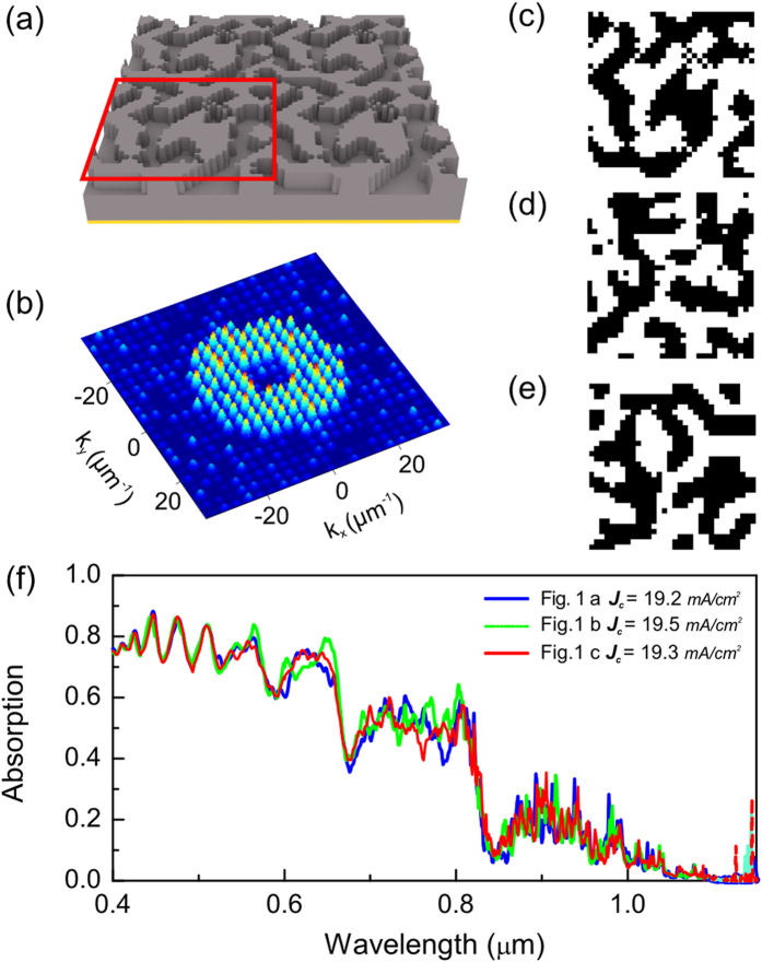
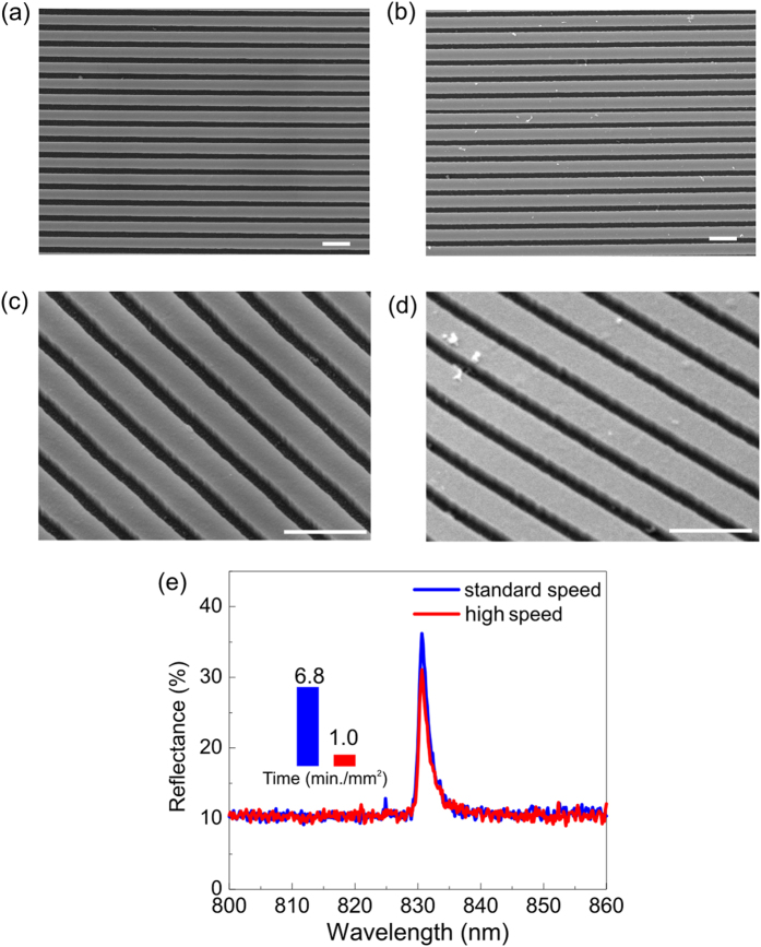
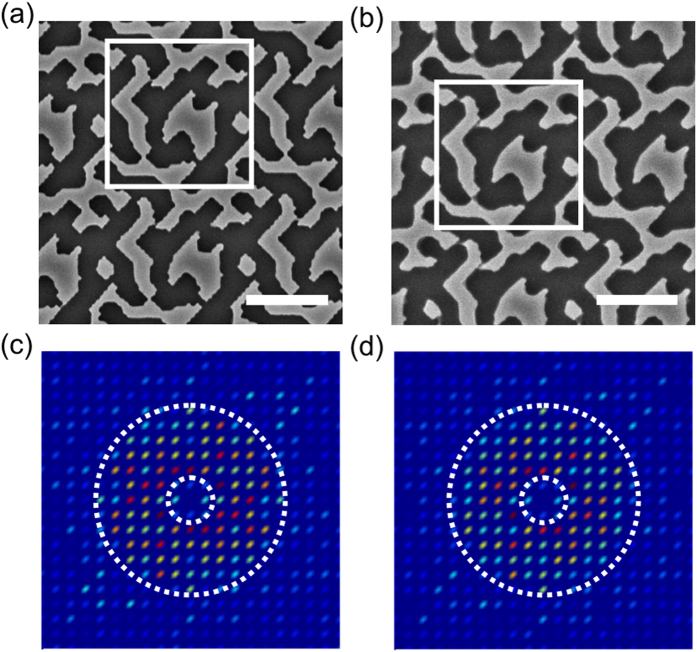
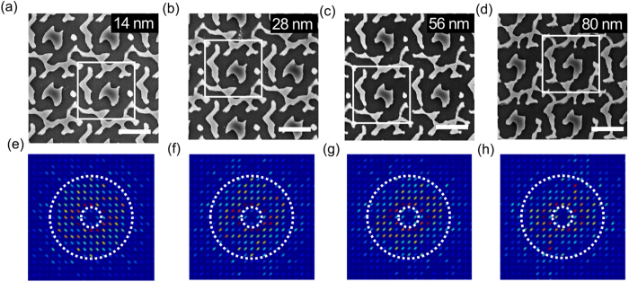
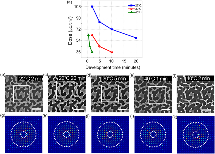
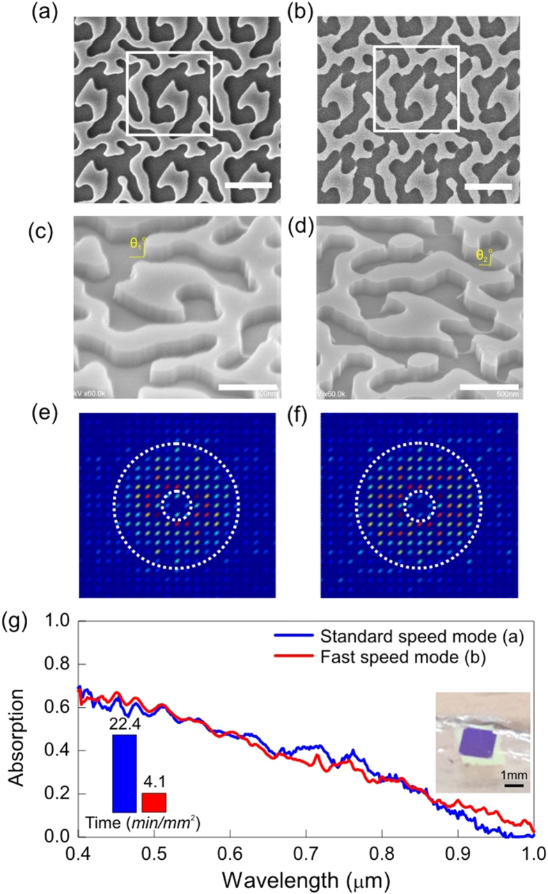
Photonic nanostructures are used for many optical systems and applications. However, some high-end applications require the use of electron-beam lithography (EBL) to generate such nanostructures. An important technological bottleneck is the exposure time of the EBL systems, which can exceed 24 hours per 1 cm(2). Here, we have developed a method based on a target function to systematically increase the writing speed of EBL. As an example, we use as the target function the fidelity of the Fourier Transform spectra of nanostructures that are designed for thin film light trapping applications, and optimize the full parameter space of the lithography process. Finally, we are able to reduce the exposure time by a factor of 5.5 without loss of photonic performance. We show that the performances of the fastest written structures are identical to the original ones within experimental error. As the target function can be varied according to different purposes, the method is also applicable to guided mode resonant grating and many other areas. These findings contribute to the advancement of EBL and point towards making the technology more attractive for commercial applications.

摘要

光子纳米结构被广泛应用于各种光学系统和领域。然而,一些高端应用需要使用电子束光刻(EBL)来生成这些纳米结构。其中一个重要的技术瓶颈是 EBL 系统的曝光时间,每 1cm² 可能需要超过 24 小时。在这里,我们基于目标函数开发了一种方法,可以系统地提高 EBL 的写入速度。例如,我们将薄膜光捕获应用设计的纳米结构傅里叶变换光谱的保真度作为目标函数,并优化光刻过程的全参数空间。最终,我们能够将曝光时间缩短 5.5 倍,而不会损失光子性能。我们证明,在实验误差范围内,最快写入结构的性能与原始结构完全相同。由于目标函数可以根据不同的目的进行调整,因此该方法也适用于导模共振光栅和许多其他领域。这些发现推动了 EBL 的发展,并使得该技术在商业应用中更具吸引力。

https://cdn.ncbi.nlm.nih.gov/pmc/blobs/78b7/5025733/fd6b957068dd/srep32945-f6.jpg
https://cdn.ncbi.nlm.nih.gov/pmc/blobs/78b7/5025733/89fdd75048be/srep32945-f1.jpg
https://cdn.ncbi.nlm.nih.gov/pmc/blobs/78b7/5025733/01452cd448ef/srep32945-f2.jpg
https://cdn.ncbi.nlm.nih.gov/pmc/blobs/78b7/5025733/54ff589c8df2/srep32945-f3.jpg
https://cdn.ncbi.nlm.nih.gov/pmc/blobs/78b7/5025733/a59df8f171b0/srep32945-f4.jpg
https://cdn.ncbi.nlm.nih.gov/pmc/blobs/78b7/5025733/8934e317ca9a/srep32945-f5.jpg
https://cdn.ncbi.nlm.nih.gov/pmc/blobs/78b7/5025733/fd6b957068dd/srep32945-f6.jpg

相似文献

1
High speed e-beam writing for large area photonic nanostructures - a choice of parameters.高速电子束直写大面积光子纳米结构 - 参数选择。
Sci Rep. 2016 Sep 16;6:32945. doi: 10.1038/srep32945.
2
Resists for sub-20-nm electron beam lithography with a focus on HSQ: state of the art.聚焦于HSQ的用于低于20纳米电子束光刻的抗蚀剂:现状
Nanotechnology. 2009 Jul 22;20(29):292001. doi: 10.1088/0957-4484/20/29/292001. Epub 2009 Jul 1.
3
Impact of electron-beam lithography irregularities across millimeter-scale resonant grating filter performances.电子束光刻不规则性对毫米级共振光栅滤波器性能的影响。
Appl Opt. 2010 Feb 1;49(4):658-62. doi: 10.1364/AO.49.000658.
4
On the reproducibility of electron-beam lithographic fabrication of photonic nanostructures.关于光子纳米结构电子束光刻制造的可重复性
Sci Rep. 2024 Apr 15;14(1):8703. doi: 10.1038/s41598-024-58842-w.
5
Advanced metal nanostructure design for surface plasmon photonic bandgap biosensor device.
Conf Proc IEEE Eng Med Biol Soc. 2006;Suppl:6521-4. doi: 10.1109/IEMBS.2006.260869.
6
Solvent-Free Nanofabrication Based on Ice-Assisted Electron-Beam Lithography.基于冰辅助电子束光刻的无溶剂纳米制造
Nano Lett. 2020 Dec 9;20(12):8841-8846. doi: 10.1021/acs.nanolett.0c03809. Epub 2020 Nov 13.
7
Reliable Nanofabrication of Single-Crystal Diamond Photonic Nanostructures for Nanoscale Sensing.用于纳米级传感的单晶金刚石光子纳米结构的可靠纳米制造。
Micromachines (Basel). 2019 Oct 24;10(11):718. doi: 10.3390/mi10110718.
8
Integration of plant viruses in electron beam lithography nanostructures.植物病毒在电子束光刻纳米结构中的整合。
Nanotechnology. 2013 Mar 15;24(10):105305. doi: 10.1088/0957-4484/24/10/105305. Epub 2013 Feb 22.
9
E-beam lithography for micro-nanofabrication.电子束光刻技术在微纳制造中的应用。
Biomicrofluidics. 2010 Jun 15;4(2):026503. doi: 10.1063/1.3437589.
10
Maskless multiple-beam laser lithography for large-area nanostructure/microstructure fabrication.用于大面积纳米结构/微结构制造的无掩膜多光束激光光刻技术。
Appl Opt. 2011 Dec 10;50(35):6536-42. doi: 10.1364/AO.50.006536.

引用本文的文献

1
Inverse design and optical vortex manipulation for thin-film absorption enhancement.用于增强薄膜吸收的逆设计与光学涡旋操控
Nanophotonics. 2023 Oct 26;12(22):4239-4254. doi: 10.1515/nanoph-2023-0583. eCollection 2023 Nov.
2
Small Feature-Size Transistors Based on Low-Dimensional Materials: From Structure Design to Nanofabrication Techniques.基于低维材料的小特征尺寸晶体管:从结构设计到纳米制造技术
Adv Sci (Weinh). 2024 Sep;11(33):e2400500. doi: 10.1002/advs.202400500. Epub 2024 Jun 17.
3
Scalable Fabrication of Metallic Nanogaps at the Sub-10 nm Level.

本文引用的文献

1
Spatial resolution effect of light coupling structures.光耦合结构的空间分辨率效应
Sci Rep. 2015 Dec 18;5:18500. doi: 10.1038/srep18500.
2
Spatial Resolution and Refractive Index Contrast of Resonant Photonic Crystal Surfaces for Biosensing.用于生物传感的共振光子晶体表面的空间分辨率和折射率对比度
IEEE Photonics J. 2015 Jun 1;7(3):6801810. doi: 10.1109/JPHOT.2015.2435699.
3
Light Management with Nanostructures for Optoelectronic Devices.用于光电器件的纳米结构光管理
在亚 10nm 级别下可扩展的金属纳米间隙制造。
Adv Sci (Weinh). 2021 Dec;8(24):e2102756. doi: 10.1002/advs.202102756. Epub 2021 Oct 31.
4
Dewetting behavior of Ge layers on SiO under annealing.退火条件下锗层在二氧化硅上的去湿行为。
Sci Rep. 2020 Aug 13;10(1):13759. doi: 10.1038/s41598-020-70723-6.
5
Chirped guided-mode resonance biosensor.啁啾导模共振生物传感器。
Optica. 2017 Feb 13;4(2):229-234. doi: 10.1364/OPTICA.4.000229. eCollection 2017 Feb 20.
6
Concurrent design of quasi-random photonic nanostructures.准随机光子纳米结构的协同设计。
Proc Natl Acad Sci U S A. 2017 Aug 15;114(33):8734-8739. doi: 10.1073/pnas.1704711114. Epub 2017 Jul 31.
J Phys Chem Lett. 2014 Apr 17;5(8):1479-95. doi: 10.1021/jz500306f. Epub 2014 Apr 8.
4
Revealing Invisible Photonic Inscriptions: Images from Strain.揭示不可见的光子印记:应变产生的图像
ACS Appl Mater Interfaces. 2015 Jun 24;7(24):13497-502. doi: 10.1021/acsami.5b02768. Epub 2015 Jun 12.
5
High speed e-beam lithography for gold nanoarray fabrication and use in nanotechnology.高速电子束光刻技术在金纳米阵列制造及其在纳米技术中的应用。
Beilstein J Nanotechnol. 2014 Oct 30;5:1918-25. doi: 10.3762/bjnano.5.202. eCollection 2014.
6
How to assess light trapping structures versus a Lambertian Scatterer for solar cells?如何评估用于太阳能电池的光捕获结构与朗伯散射体?
Opt Express. 2014 Mar 10;22 Suppl 2:A542-51. doi: 10.1364/OE.22.00A542.
7
Position-controlled uniform GaAs nanowires on silicon using nanoimprint lithography.采用纳米压印光刻技术在硅衬底上制备位置可控的均匀 GaAs 纳米线。
Nano Lett. 2014 Feb 12;14(2):960-6. doi: 10.1021/nl404376m. Epub 2014 Jan 29.
8
Silicon nanostructures for photonics and photovoltaics.硅纳米结构用于光子学和光伏技术。
Nat Nanotechnol. 2014 Jan;9(1):19-32. doi: 10.1038/nnano.2013.271.
9
Deterministic quasi-random nanostructures for photon control.用于光子控制的确定性类随机纳米结构。
Nat Commun. 2013;4:2665. doi: 10.1038/ncomms3665.
10
Efficient light trapping in inverted nanopyramid thin crystalline silicon membranes for solar cell applications.用于太阳能电池的倒置纳米金字塔型薄晶体硅膜中的高效光捕获。
Nano Lett. 2012 Jun 13;12(6):2792-6. doi: 10.1021/nl2045777. Epub 2012 May 29.