Nanotechnology Laboratory, School of Engineering, University of Birmingham, Birmingham B15 2TT, UK.
Nanoscale. 2017 Jan 7;9(1):266-276. doi: 10.1039/c6nr07841a. Epub 2016 Dec 1.
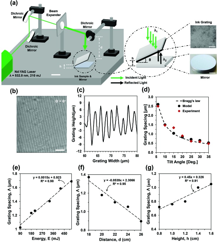
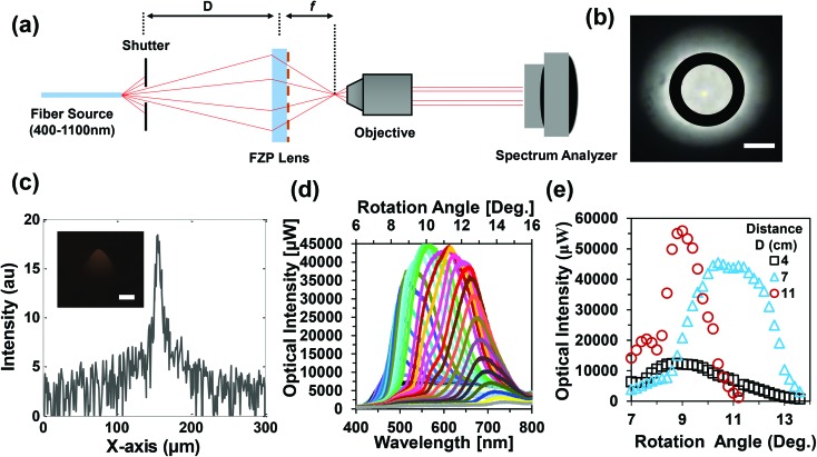
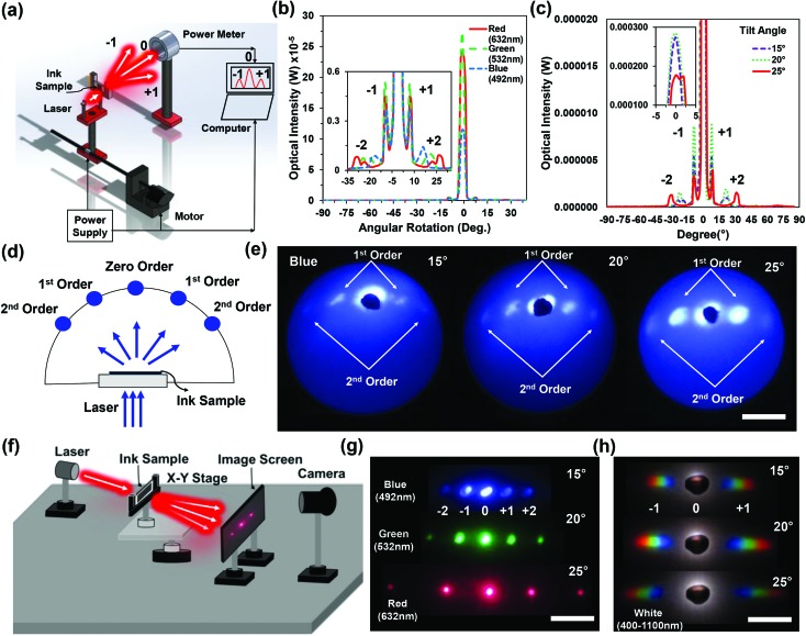
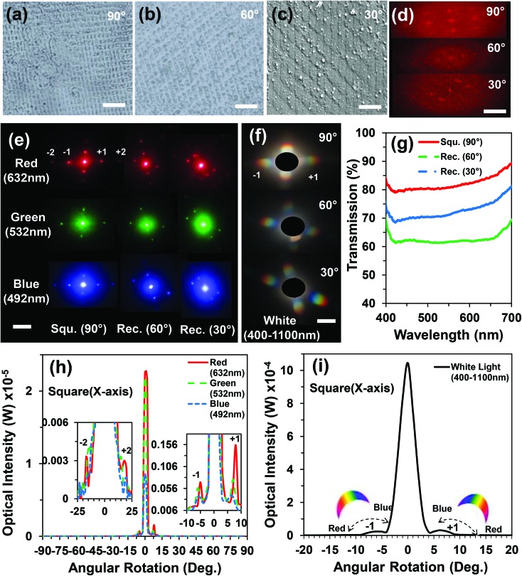
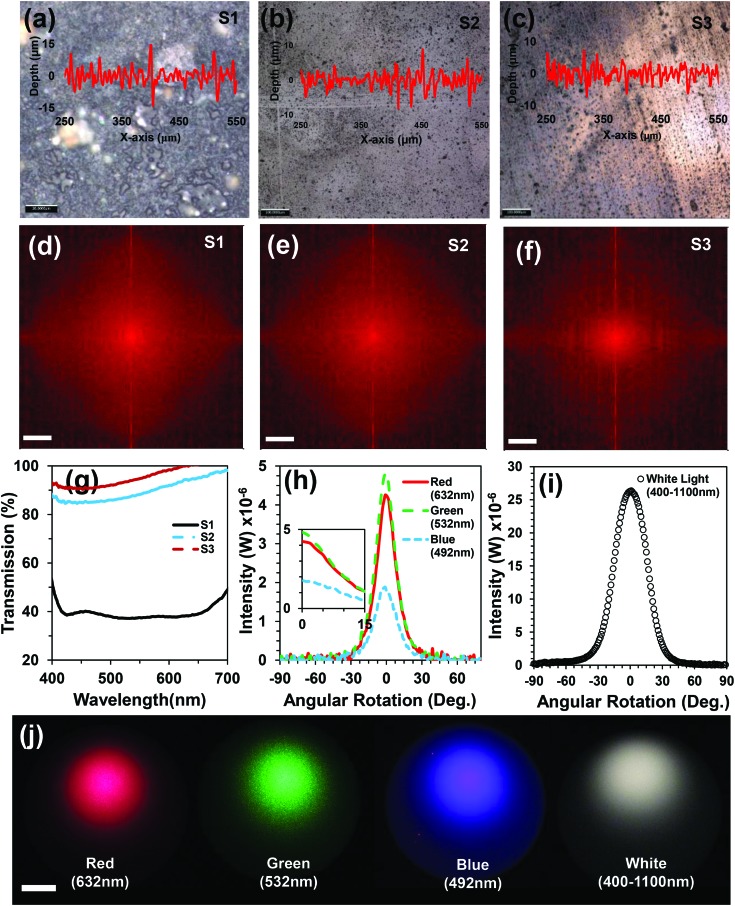
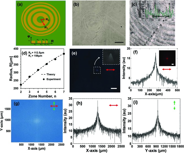
Advances in holography have led to applications including data storage, displays, security labels, and colorimetric sensors. However, existing top-down approaches for the fabrication of holographic devices are complex, expensive, and expertise dependent, limiting their use in practical applications. Here, ink-based holographic devices have been created for a wide range of applications in diffraction optics. A single pulse of a 3.5 ns Nd:YAG laser allowed selective ablation of ink to nanofabricate planar optical devices. The practicality of this method is demonstrated by fabricating ink-based diffraction gratings, 2D holographic patterns, optical diffusers, and Fresnel zone plate (FZP) lenses by using the ink. The fabrication processes were rationally designed using predictive computational modeling and the devices were fabricated within a few minutes demonstrating amenability for large scale printable optics through industrial manufacturing. It is anticipated that ink will be a promising diffraction optical material for the rapid printing of low-cost planar nanophotonic devices.
全息术的进展已经带来了包括数据存储、显示、安全标签和比色传感器在内的应用。然而,现有的用于制造全息设备的自上而下的方法复杂、昂贵且依赖专业知识,限制了它们在实际应用中的使用。在这里,基于墨水的全息设备已经在衍射光学中得到了广泛的应用。通过使用 3.5ns Nd:YAG 激光的单个脉冲,可以选择性地烧蚀墨水来纳米制造平面光器件。通过使用墨水,制造基于墨水的衍射光栅、二维全息图案、光学扩散器和菲涅耳波带片 (FZP) 透镜,证明了这种方法的实用性。使用预测计算建模合理设计了制造工艺,并且在几分钟内制造出了设备,这表明通过工业制造可以实现大规模可打印光学器件的适用性。预计墨水将成为一种有前途的衍射光学材料,可用于快速打印低成本平面纳米光子器件。