AlQattan Bader, Butt Haider, Sabouri Aydin, Yetisen Ali K, Ahmed Rajib, Mahmoodi Nasim
Nanotechnology Laboratory, School of Engineering, University of Birmingham, Birmingham B15 2TT, UK. Email:
Harvard Medical School and Wellman Center for Photomedicine, Massachusetts General Hospital, 65 Landsdowne Street, Cambridge, MA 02139, USA; Harvard-MIT Division of Health Sciences and Technology, Massachusetts Institute of Technology, Cambridge, MA 02139, USA.
RSC Adv. 2016 Dec 4;6(112):111269-111275. doi: 10.1039/c6ra22241b. Epub 2016 Nov 22.
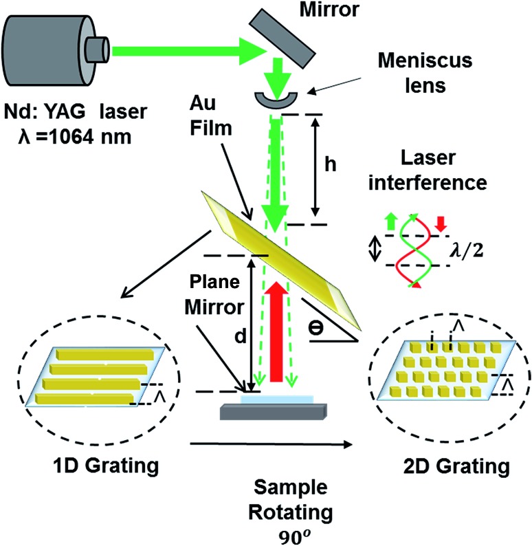
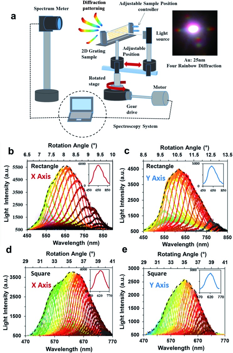
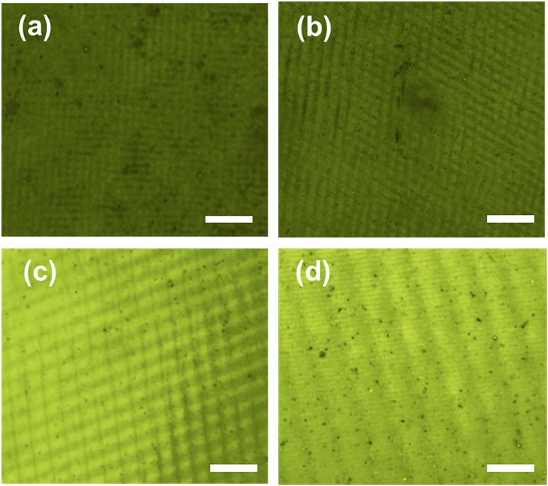
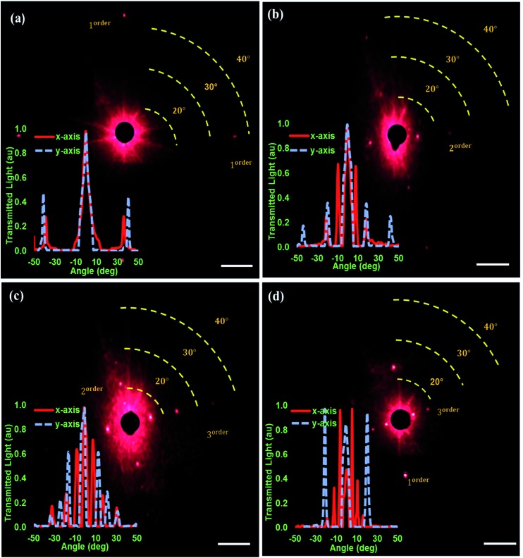
The development of accurate and rapid techniques to produce nanophotonic structures is essential in data storage, sensors, and spectroscopy. Existing bottom-up and top-down approaches to fabricate nanophotonic devices are high cost and time consuming, limiting their mass manufacturing and practical applications. Here, we demonstrate a strategy to rapidly create 25-40 nm thick 1/2D Au-Ti nanopatterns using holographic direct laser interference patterning (DLIP). Pulses of an Nd:YAG laser (1064 nm) in holographic Denisyuk reflection mode were used to create ablative interference fringes. The constructive interference antinode regions of the standing wave selectively ablated a Au-Ti layer in localized regions to controllably form nanogratings. Varying the laser exposure parameters allowed for rapid patterning of 2D square and rectangular arrays within seconds. Controlling the distances between the laser source, recording medium, and the object, allowed for achieving a 2D spatial grating periodicity of 640 nm × 640 nm. Diffracted and transmitted light spectra of 2D nanostructure arrays were analyzed using angle-resolved measurements and spectroscopy.
开发精确且快速的技术来制造纳米光子结构对于数据存储、传感器和光谱学至关重要。现有的制造纳米光子器件的自下而上和自上而下方法成本高且耗时,限制了它们的大规模制造和实际应用。在此,我们展示了一种使用全息直接激光干涉光刻(DLIP)快速创建25 - 40纳米厚的1/2D金 - 钛纳米图案的策略。在全息德尼苏克反射模式下,使用Nd:YAG激光(1064纳米)脉冲来创建烧蚀干涉条纹。驻波的相长干涉波腹区域在局部区域选择性地烧蚀金 - 钛层,以可控方式形成纳米光栅。改变激光曝光参数可在数秒内快速对二维正方形和矩形阵列进行图案化。控制激光源、记录介质和物体之间的距离,可实现640纳米×640纳米的二维空间光栅周期。使用角度分辨测量和光谱学分析了二维纳米结构阵列的衍射光和透射光谱。