Dipartimento di Scienze di Base ed Applicate per l'Ingegneria, Sapienza Università di Roma, A. Scarpa 16, 00161, Rome, Italy.
Optoelectronics Research Centre, Tampere University of Technology, Korkeakoulunkatu 3, 33720, Tampere, Finland.
Sci Rep. 2017 Jun 6;7(1):2833. doi: 10.1038/s41598-017-02839-1.
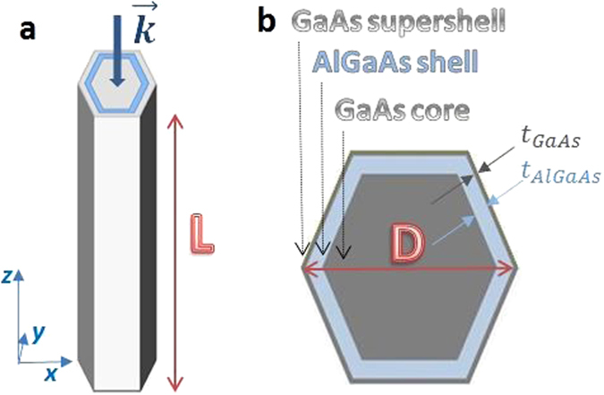
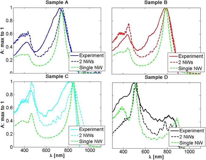
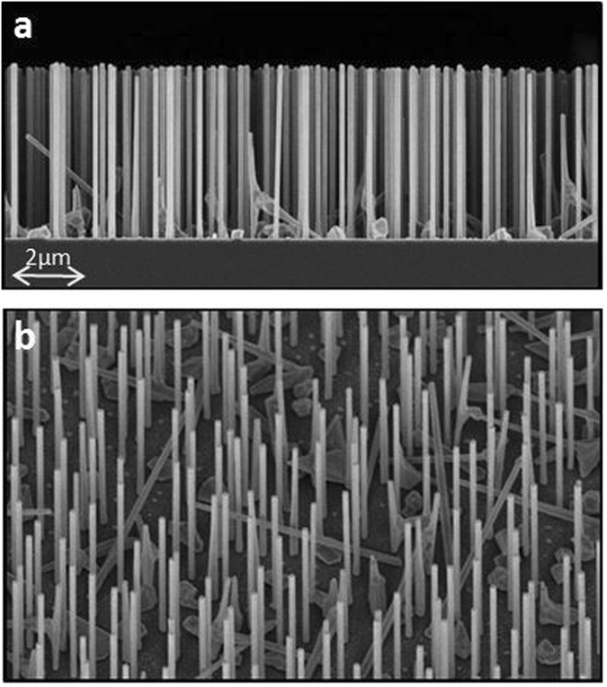
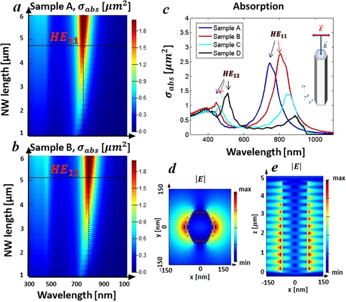
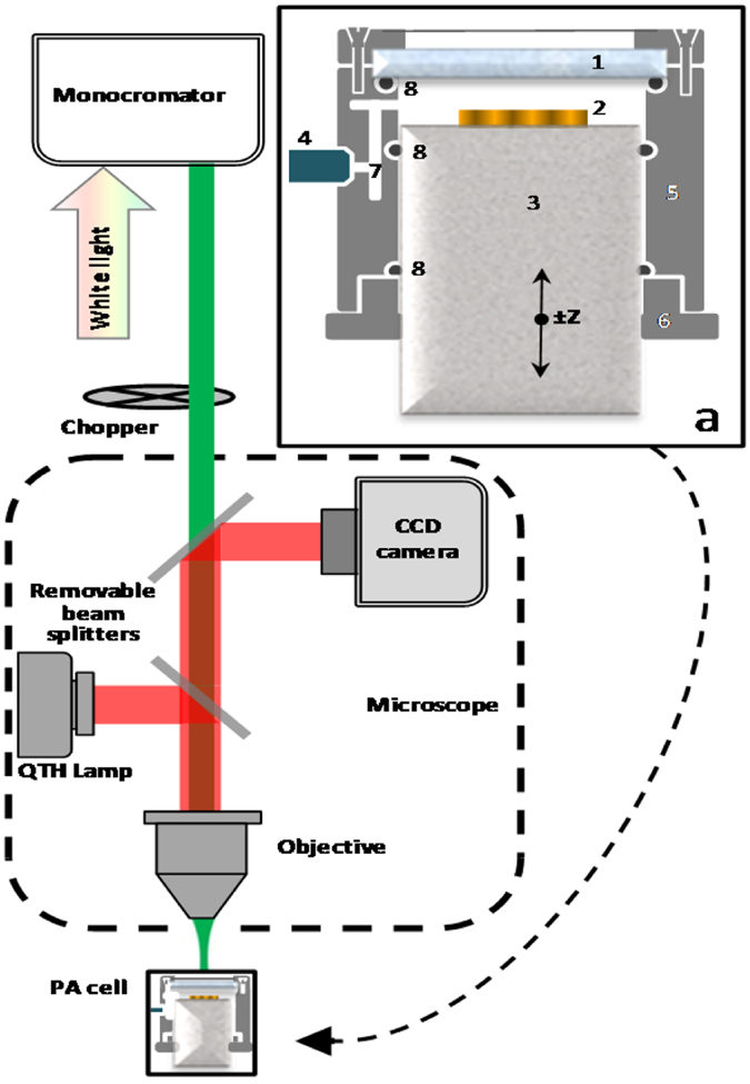
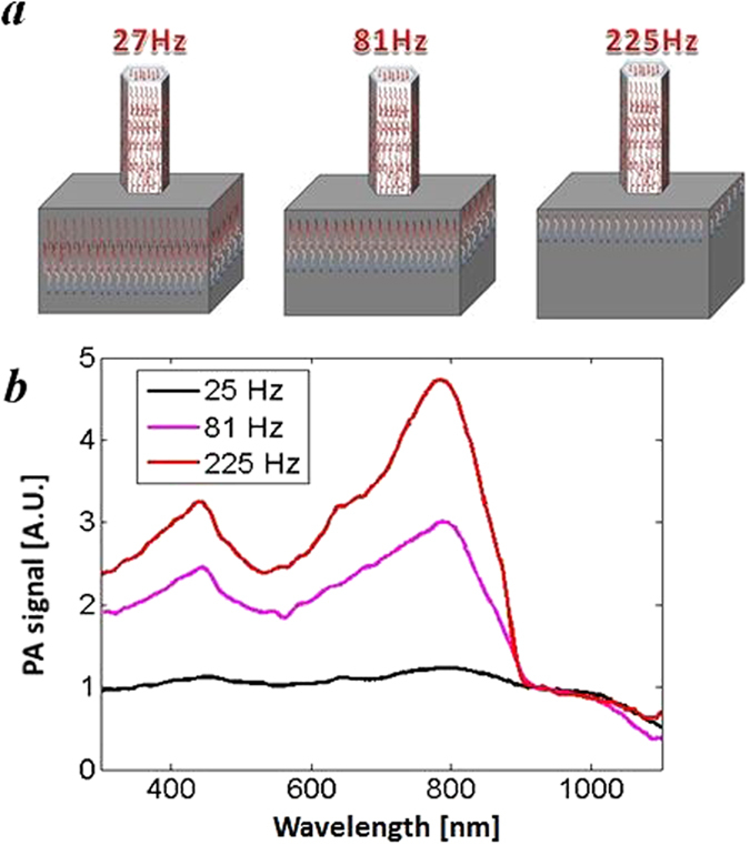
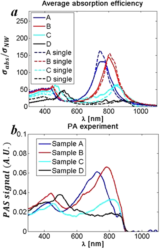
III-V semiconductors nanowires (NW) have recently attracted a significant interest for their potential application in the development of high efficiency, highly-integrated photonic devices and in particular for the possibility to integrate direct bandgap materials with silicon-based devices. Here we report the absorbance properties of GaAs-AlGaAs-GaAs core-shell-supershell NWs using photo-acoustic spectroscopy (PAS) measurements in the spectral range from 300 nm to 1100 nm wavelengths. The NWs were fabricated by self-catalyzed growth on Si substrates and their dimensions (length ~5 μm, diameter ~140-150 nm) allow for the coupling of the incident light to the guided modes in near-infrared (IR) part of the spectrum. This coupling results in resonant absorption peaks in the visible and near IR clearly evidenced by PAS. The analysis reveal broadening of the resonant absorption peaks arising from the NW size distribution and the interaction with other NWs. The results show that the PAS technique, directly providing scattering independent absorption spectra, is a very useful tool for the characterization and investigation of vertical NWs as well as for the design of NW ensembles for photonic applications, such as Si-integrated light sources, solar cells, and wavelength dependent photodetectors.
III-V 族半导体纳米线 (NW) 最近因其在开发高效、高集成光子器件方面的潜在应用而引起了极大的关注,特别是因为有可能将直接带隙材料与基于硅的器件集成。在这里,我们使用光声光谱 (PAS) 测量报告了 GaAs-AlGaAs-GaAs 核壳超壳 NWs 的吸收特性,测量波长范围为 300nm 至 1100nm。NWs 是在 Si 衬底上自催化生长而成的,其尺寸(长度约为 5μm,直径约为 140-150nm)允许将入射光耦合到近红外 (IR) 光谱的导模中。这种耦合导致在可见和近红外部分出现共振吸收峰,PAS 清楚地证明了这一点。分析表明,由于 NW 尺寸分布和与其他 NW 的相互作用,共振吸收峰的展宽。结果表明,PAS 技术直接提供与散射无关的吸收光谱,是表征和研究垂直 NW 以及设计用于光子应用的 NW 组件的非常有用的工具,例如硅集成光源、太阳能电池和波长相关光电探测器。