• 文献检索
  • 文档翻译
  • 深度研究
  • 学术资讯
  • Suppr Zotero 插件Zotero 插件
  • 邀请有礼
  • 套餐&价格
  • 历史记录
应用&插件
Suppr Zotero 插件Zotero 插件浏览器插件Mac 客户端Windows 客户端微信小程序
定价
高级版会员购买积分包购买API积分包
服务
文献检索文档翻译深度研究API 文档MCP 服务
关于我们
关于 Suppr公司介绍联系我们用户协议隐私条款
关注我们

Suppr 超能文献

核心技术专利:CN118964589B侵权必究
粤ICP备2023148730 号-1Suppr @ 2026

文献检索

告别复杂PubMed语法,用中文像聊天一样搜索,搜遍4000万医学文献。AI智能推荐,让科研检索更轻松。

立即免费搜索

文件翻译

保留排版,准确专业,支持PDF/Word/PPT等文件格式,支持 12+语言互译。

免费翻译文档

深度研究

AI帮你快速写综述,25分钟生成高质量综述,智能提取关键信息,辅助科研写作。

立即免费体验

基于并五苯的薄膜晶体管栅极绝缘体的聚(4-乙烯基苯酚)交联过程中快速低功率微波感应加热方案的研究

Investigation of Rapid Low-Power Microwave-Induction Heating Scheme on the Cross-Linking Process of the Poly(4-vinylphenol) for the Gate Insulator of Pentacene-Based Thin-Film Transistors.

作者信息

Fan Ching-Lin, Shang Ming-Chi, Wang Shea-Jue, Hsia Mao-Yuan, Lee Win-Der, Huang Bohr-Ran

机构信息

Graduate Institute of Electro-Optical Engineering, National Taiwan University of Science and Technology, 43 Sec. 4, Keelung Road, Taipei 106, Taiwan.

Department of Electronic Engineering, National Taiwan University of Science and Technology, 43 Sec. 4, Keelung Road, Taipei 106, Taiwan.

出版信息

Materials (Basel). 2017 Jul 3;10(7):742. doi: 10.3390/ma10070742.

DOI:10.3390/ma10070742
PMID:28773101
原文链接:https://pmc.ncbi.nlm.nih.gov/articles/PMC5551785/
Abstract

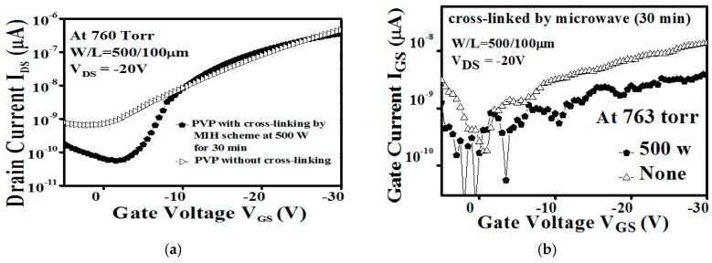
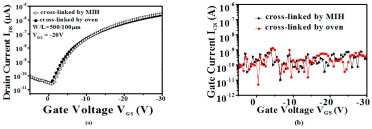
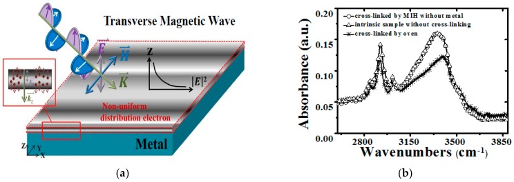
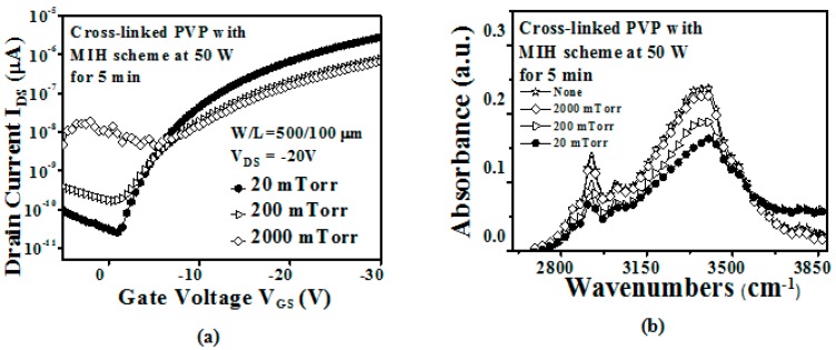
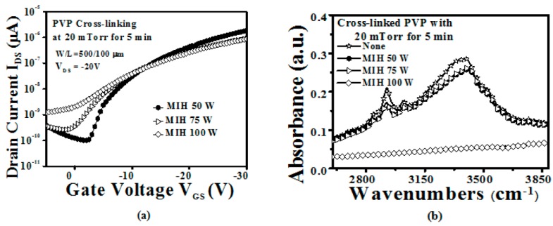
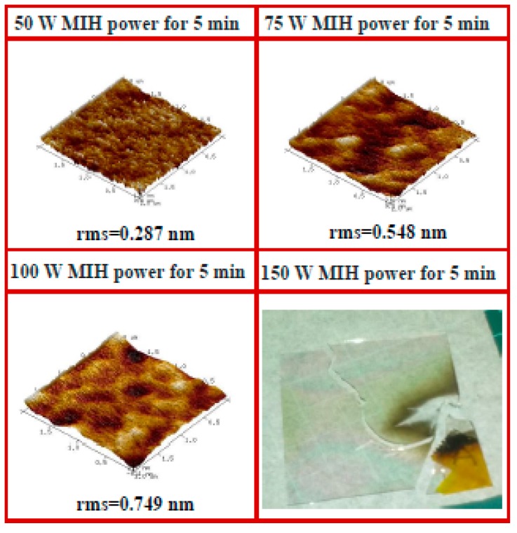
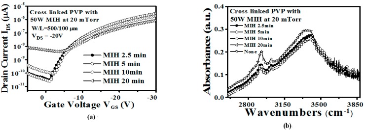
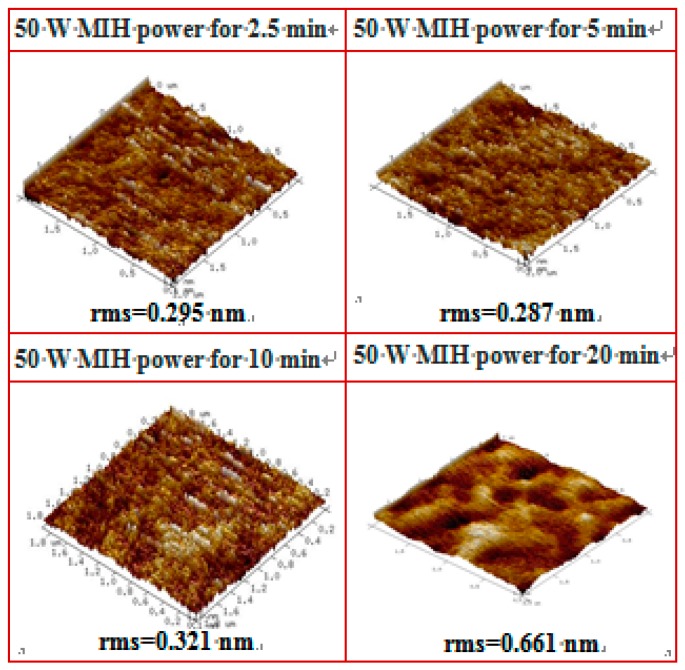
In this study, a proposed Microwave-Induction Heating (MIH) scheme has been systematically studied to acquire suitable MIH parameters including chamber pressure, microwave power and heating time. The proposed MIH means that the thin indium tin oxide (ITO) metal below the Poly(4-vinylphenol) (PVP) film is heated rapidly by microwave irradiation and the heated ITO metal gate can heat the PVP gate insulator, resulting in PVP cross-linking. It is found that the attenuation of the microwave energy decreases with the decreasing chamber pressure. The optimal conditions are a power of 50 W, a heating time of 5 min, and a chamber pressure of 20 mTorr. When suitable MIH parameters were used, the effect of PVP cross-linking and the device performance were similar to those obtained using traditional oven heating, even though the cross-linking time was significantly decreased from 1 h to 5 min. Besides the gate leakage current, the interface trap state density (Nit) was also calculated to describe the interface status between the gate insulator and the active layer. The lowest interface trap state density can be found in the device with the PVP gate insulator cross-linked by using the optimal MIH condition. Therefore, it is believed that the MIH scheme is a good candidate to cross-link the PVP gate insulator for organic thin-film transistor applications as a result of its features of rapid heating (5 min) and low-power microwave-irradiation (50 W).

摘要

在本研究中,对一种提出的微波感应加热(MIH)方案进行了系统研究,以获取合适的MIH参数,包括腔室压力、微波功率和加热时间。所提出的MIH是指聚(4-乙烯基苯酚)(PVP)薄膜下方的薄氧化铟锡(ITO)金属通过微波辐射快速加热,加热后的ITO金属栅极可加热PVP栅极绝缘体,从而导致PVP交联。发现微波能量的衰减随着腔室压力的降低而减小。最佳条件是功率为50 W、加热时间为5分钟、腔室压力为20毫托。当使用合适的MIH参数时,PVP交联效果和器件性能与使用传统烘箱加热时相似,尽管交联时间从1小时显著缩短至5分钟。除了栅极漏电流外,还计算了界面陷阱态密度(Nit)来描述栅极绝缘体与有源层之间的界面状态。在采用最佳MIH条件交联PVP栅极绝缘体的器件中可发现最低的界面陷阱态密度。因此,由于其快速加热(5分钟)和低功率微波辐射(50 W)的特点,相信MIH方案是用于有机薄膜晶体管应用中交联PVP栅极绝缘体的良好候选方案。

https://cdn.ncbi.nlm.nih.gov/pmc/blobs/d4a9/5551785/c1dfc90b9d4e/materials-10-00742-g008.jpg
https://cdn.ncbi.nlm.nih.gov/pmc/blobs/d4a9/5551785/6c23dbdddcb0/materials-10-00742-g001.jpg
https://cdn.ncbi.nlm.nih.gov/pmc/blobs/d4a9/5551785/7438da3d1a50/materials-10-00742-g002.jpg
https://cdn.ncbi.nlm.nih.gov/pmc/blobs/d4a9/5551785/6da5bb16b80f/materials-10-00742-g003.jpg
https://cdn.ncbi.nlm.nih.gov/pmc/blobs/d4a9/5551785/793d4178a133/materials-10-00742-g004.jpg
https://cdn.ncbi.nlm.nih.gov/pmc/blobs/d4a9/5551785/d4b6b723f15f/materials-10-00742-g005.jpg
https://cdn.ncbi.nlm.nih.gov/pmc/blobs/d4a9/5551785/1f6415bb4ce2/materials-10-00742-g006.jpg
https://cdn.ncbi.nlm.nih.gov/pmc/blobs/d4a9/5551785/e5b38d0f25b6/materials-10-00742-g007.jpg
https://cdn.ncbi.nlm.nih.gov/pmc/blobs/d4a9/5551785/c1dfc90b9d4e/materials-10-00742-g008.jpg

相似文献

1
Investigation of Rapid Low-Power Microwave-Induction Heating Scheme on the Cross-Linking Process of the Poly(4-vinylphenol) for the Gate Insulator of Pentacene-Based Thin-Film Transistors.基于并五苯的薄膜晶体管栅极绝缘体的聚(4-乙烯基苯酚)交联过程中快速低功率微波感应加热方案的研究
Materials (Basel). 2017 Jul 3;10(7):742. doi: 10.3390/ma10070742.
2
Performance Enhancement of Pentacene-Based Organic Thin-Film Transistors Using a High-K PVA/Low-K PVP Bilayer as the Gate Insulator.使用高介电常数聚乙烯醇/低介电常数聚乙烯吡咯烷酮双层作为栅极绝缘体提高并五苯有机薄膜晶体管的性能
Polymers (Basel). 2021 Nov 15;13(22):3941. doi: 10.3390/polym13223941.
3
Stability Study of Flexible 6,13-Bis(triisopropylsilylethynyl)pentacene Thin-Film Transistors with a Cross-Linked Poly(4-vinylphenol)/Yttrium Oxide Nanocomposite Gate Insulator.具有交联聚(4-乙烯基苯酚)/氧化钇纳米复合栅极绝缘体的柔性6,13-双(三异丙基甲硅烷基乙炔基)并五苯薄膜晶体管的稳定性研究
Polymers (Basel). 2016 Mar 16;8(3):88. doi: 10.3390/polym8030088.
4
Instantaneous Pulsed-Light Cross-Linking of a Polymer Gate Dielectric for Flexible Organic Thin-Film Transistors.用于柔性有机薄膜晶体管的聚合物栅介质的瞬时脉冲光交联。
ACS Appl Mater Interfaces. 2017 Apr 5;9(13):11721-11731. doi: 10.1021/acsami.6b14957. Epub 2017 Mar 27.
5
Additive effect of poly(4-vinylphenol) gate dielectric in organic thin film transistor at low temperature process.聚(4-乙烯基苯酚)栅极电介质在低温工艺有机薄膜晶体管中的加和效应。
J Nanosci Nanotechnol. 2013 May;13(5):3313-6. doi: 10.1166/jnn.2013.7272.
6
High performance flexible organic thin film transistors (OTFTs) with octadecyltrichlorsilane/ Al2O3/poly(4-vinylphenol) multilayer insulators.具有十八烷基三氯硅烷/Al2O3/聚(4-乙烯基苯酚)多层绝缘体的高性能柔性有机薄膜晶体管
J Nanosci Nanotechnol. 2012 Feb;12(2):1348-52. doi: 10.1166/jnn.2012.4695.
7
Study of surface-modified PVP gate dielectric in organic thin film transistors with the nano-particle silver ink source/drain electrode.具有纳米颗粒银墨源/漏电极的有机薄膜晶体管中表面改性聚乙烯吡咯烷酮栅极电介质的研究。
J Nanosci Nanotechnol. 2011 Jul;11(7):5640-4. doi: 10.1166/jnn.2011.4418.
8
Organic thin film transistors using a polyhedral oligomeric silsesquioxane-based photo-patternable insulating material.使用基于多面体低聚倍半硅氧烷的可光图案化绝缘材料的有机薄膜晶体管。
J Nanosci Nanotechnol. 2009 Dec;9(12):6923-7. doi: 10.1166/jnn.2009.1648.
9
A Low Temperature, Solution-Processed Poly(4-vinylphenol), YO(x) Nanoparticle Composite/Polysilazane Bi-Layer Gate Insulator for ZnO Thin Film Transistor.用于氧化锌薄膜晶体管的低温溶液法制备的聚(4-乙烯基苯酚)、YO(x)纳米颗粒复合材料/聚硅氮烷双层栅极绝缘体
J Nanosci Nanotechnol. 2016 Mar;16(3):2632-6. doi: 10.1166/jnn.2016.11080.
10
Low-voltage-driven pentacene thin-film transistors with cross-linked poly(4-vinylphenol)/high-k Bi55b3O15 hybrid dielectric for phototransistor.用于光电晶体管的具有交联聚(4-乙烯基苯酚)/高介电常数Bi55b3O15混合电介质的低压驱动并五苯薄膜晶体管
J Nanosci Nanotechnol. 2012 Apr;12(4):3355-9. doi: 10.1166/jnn.2012.5640.

引用本文的文献

1
The Role of Interdigitated Electrodes in Printed and Flexible Electronics.叉指电极在印刷和柔性电子学中的作用。
Sensors (Basel). 2024 Apr 24;24(9):2717. doi: 10.3390/s24092717.
2
Performance Enhancement of Pentacene-Based Organic Thin-Film Transistors Using a High-K PVA/Low-K PVP Bilayer as the Gate Insulator.使用高介电常数聚乙烯醇/低介电常数聚乙烯吡咯烷酮双层作为栅极绝缘体提高并五苯有机薄膜晶体管的性能
Polymers (Basel). 2021 Nov 15;13(22):3941. doi: 10.3390/polym13223941.
3
Sulpho-Salicylic Acid Grafted to Ferrite Nanoparticles for n-Type Organic Semiconductors.

本文引用的文献

1
Enabling gate dielectric design for all solution-processed, high-performance, flexible organic thin-film transistors.为全溶液处理的高性能柔性有机薄膜晶体管实现栅极电介质设计。
J Am Chem Soc. 2006 Apr 12;128(14):4554-5. doi: 10.1021/ja060620l.
接枝到用于n型有机半导体的铁氧体纳米颗粒上的磺基水杨酸
Nanomaterials (Basel). 2020 Sep 9;10(9):1787. doi: 10.3390/nano10091787.
4
Printed Electronics as Prepared by Inkjet Printing.通过喷墨印刷制备的印刷电子学。
Materials (Basel). 2020 Feb 4;13(3):704. doi: 10.3390/ma13030704.